
Excertos do catálogo

M41T94 Serial real-time clock with 44 bytes NVRAM and reset Features ■ Counters for tenths/hundredths of seconds, seconds, minutes, hours, day, date, month, year, and century 32 KHz crystal oscillator integrating load capacitance (12.5 pF) providing exceptional oscillator stability and high crystal series resistance operation Ultralow battery supply current of 500 nA (max) 2.5 to 5.5 V oscillator operating voltage Automatic switchover and deselect circuitry 44 bytes of general purpose RAM Programmable alarm and interrupt function (valid even during battery backup mode) Accurate programmable watchdog timer (from 62.5 ms to 128 s) Microprocessor power-on reset Choice of power-fail deselect voltages (VCC = 2.7 to 5.5 V): – THS = VSS; 2.55 V ≤ VPFD ≤ 2.70 V – THS = VCC; 4.20 V ≤ VPFD ≤ 4.50 V Packaging includes a 28-lead SOIC and SNAPHAT® top (to be ordered separately) or 16-lead SOIC 28-lead SOIC package provides direct connection for a SNAPHAT® top which contains the battery and crystal Serial peripheral interface (2 MHz SPI) RoHS compliant – Lead-free second level interconnect SNAPHAT® (SH) battery & crystal
Abrir o catálogo na página 1
Serial data input (SDI) . . . . . . . . . . . . . . . . . . . . . . . . . . . . . . . . . . . . . . . 11 Serial data output (SDO) . . . . . . . . . . . . . . . . . . . . . . . . . . . . . . . . . . . . . 11 Read and write cycles . . . . . . . . . . . . . . . . . . . . . . . . . . . . . . . . . . . . . . . 15 Data retention mode . . . . . . . . . . . . . . . . . . . . . . . . . . . . . . . . . . . . . . . . . 15 Setting alarm clock registers . . . . . . . . . . . . . . . . . . . . . . . . . . . . . . . . . . 19 Square wave output . . . . . . . . . . . . . . . . . . . . . . . . . . . . . . ....
Abrir o catálogo na página 2
List of figures Figure 1. Figure 2. Figure 3. Figure 4. Figure 5. Figure 6. Figure 7. Figure 8. Figure 9. Figure 10. Figure 11. Figure 12. Figure 13. Figure 14. Figure 15. Figure 16. Figure 17. Figure 18. Figure 19. Figure 20. Figure 21. Figure 22. Logic diagram . . . . . . . . . . . . . . . . . . . . . . . . . . . . . . . . . . . . . . . . . . . . . . . . . . . . . . . . . . . . 7 16-pin SOIC connections . . . . . . . . . . . . . . . . . . . . . . . . . . . . . . . . . . . . . . . . . . . . . . . . . . . 7 28-pin SOIC connections . . . . . . . . . . . . . . . . . . . . . . . . . . . . . ....
Abrir o catálogo na página 4
List of tables Table 1. Table 2. Table 3. Table 4. Table 5. Table 6. Table 7. Table 8. Table 9. Table 10. Table 11. Table 12. Table 13. Table 14. Table 15. Table 16. Table 17. Table 18. Table 19. Table 20. Table 21. Table 22. Signal names . . . . . . . . . . . . . . . . . . . . . . . . . . . . . . . . . . . . . . . . . . . . . . . . . . . . . . . . . . . . 8 Function table . . . . . . . . . . . . . . . . . . . . . . . . . . . . . . . . . . . . . . . . . . . . . . . . . . . . . . . . . . . 10 AC characteristics . . . . . . . . . . . . . . . . . . . . . . . . . . . . . . . . . . . . . . . . ....
Abrir o catálogo na página 5
Description The M41T94 is a serial real-time clock with 44 bytes of NVRAM and a RESET output. A built-in 32,768 Hz oscillator (external crystal controlled) and 8 bytes of the SRAM (see Table 4 on page 18) are used for the clock/calendar function and are configured in binary coded decimal (BCD) format. An additional 12 bytes of RAM provide status/control of alarm, watchdog and square wave functions. Addresses and data are transferred serially via a serial SPI interface. The built-in address register is incremented automatically after each WRITE or READ data byte. The M41T94 has a built-in...
Abrir o catálogo na página 6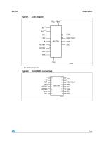
Figure 1. Logic diagram Figure 2. 16-pin SOIC connections
Abrir o catálogo na página 7
Signal names Chip enable Interrupt/frequency test/out output (open drain) Reset output (open drain) Serial clock input Serial data input Serial data output Square wave output Watchdog input Oscillator input Oscillator output Battery supply voltage Supply voltage
Abrir o catálogo na página 8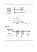
Block diagram REAL TIME CLOCK CALENDAR SQUARE WAVE 1. Open drain output Hardware hookup SPI Interface with (CPOL, CPHA)(1) = ('0','0') or ('1','1') 1. CPOL (clock polarity) and CPHA (clock phase) are bits that may be set in the SPI control register of the MCU.
Abrir o catálogo na página 9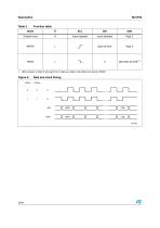
Table 2. Function table 1. SDO remains at High Z until eight bits of data are ready to be shifted out during a READ. Figure 6. Data and clock timing CPOL CPHA
Abrir o catálogo na página 10
Signal description Signal description Serial data output (SDO) The output pin is used to transfer data serially out of the memory. Data is shifted out on the falling edge of the serial clock. Serial data input (SDI) The input pin is used to transfer data serially into the device. Instructions, addresses, and the data to be written, are each received this way. Input is latched on the rising edge of the serial clock. Serial clock (SCL) The serial clock provides the timing for the serial interface (as shown in Figure 7 on page 13 and Figure 8 on page 14). The W/R bit, addresses, or data are...
Abrir o catálogo na página 11
Operation The M41T94 clock operates as a slave device on the SPI serial bus. Each memory device is accessed by a simple serial interface that is SPI bus compatible. The bus signals are SCL, SDI and SDO (see Table 1 on page 8 and Figure 5 on page 9). The device is selected when the chip enable input (E) is held low. All instructions, addresses and data are shifted serially in and out of the chip. The most significant bit is presented first, with the data input (SDI) sampled on the first rising edge of the clock (SCL) after the chip enable (E) goes low. The 64 bytes contained in the device...
Abrir o catálogo na página 12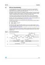
SPI bus characteristics The serial peripheral interface (SPI) bus is intended for synchronous communication between different ICs. It consists of four signal lines: serial data input (SDI), serial data output (SDO), serial clock (SCL) and a chip enable (E). By definition a device that gives out a message is called “transmitter,” the receiving device that gets the message is called “receiver.” The device that controls the message is called “master.” The devices that are controlled by the master are called “slaves.” The E input is used to initiate and terminate a data transfer. The SCL input...
Abrir o catálogo na página 13Todos os catálogos e folhetos técnicos STMicroelectronics
-
 STGW30NC60KD
14 Páginas
-
 STGB14NC60K STGD14NC60K
16 Páginas
-
 HD1750FX
8 Páginas
-
 TDA75610SLV
42 Páginas
-
 TDA7391
13 Páginas
-
 TDA7376B
15 Páginas
-
 TDA7375V
15 Páginas
-
 TDA2005
25 Páginas
-
 L4989D, L4989MD
19 Páginas
-
 L4938ED L4938EPD
20 Páginas
-
 L4949ED-E L4949EP-E
19 Páginas
-
 L4925
L492514 Páginas
-
 FDA903U
80 Páginas
-
 FDA803U
76 Páginas
-
 FDA903D
82 Páginas
-
 FDA803D
78 Páginas
-
 BALF-SPI2-02D3
13 Páginas
-
 LIS2DTW12
65 Páginas
-
 VL53L0X
40 Páginas
-
 LPS22HH
59 Páginas
-
 Standard products offer overview
13 Páginas
-
 M40SZ100W
20 Páginas
-
 A1C15S12M3
17 Páginas
-
 TSX923
32 Páginas
-
 TS1851
24 Páginas
-
 LMV321
17 Páginas
-
 TDA7303audio processor with loudness
20 Páginas
-
 Micro-sized Bluetooth® modules
4 Páginas
-
 Products and solutions for solar energy
28 Páginas
-
 SPC56 MCU family development tools
8 Páginas
-
 E-meter single-phase combo solution
4 Páginas
-
 Smart grid distribution and smart meters
20 Páginas
-
 Serial real-time clock (RTC) ICs
16 Páginas
-
 Advanced door electronics solutions
20 Páginas
-
 FFX: Full flexible amplification
7 Páginas
-
 TDA2003LG 10 W CAR AUDIO amplifier
8 Páginas
-
 TDA2003LG
8 Páginas
-
 L272 Dual Power Operational Amplifier
10 Páginas
-
 HCF4541 Programmable Timer
10 Páginas
-
 STA8058 GPS multi-chip module
14 Páginas
-
 TDA7410ND Signal Processor
34 Páginas
-
 TDA7410ND Signal Processor
34 Páginas
-
 TSA1204 DUAL CHANNEL
31 Páginas


Catálogos arquivados
-
 NEATSwitch
6 Páginas
-
 Power MOSFETs for metering
2 Páginas


