
Excertos do catálogo
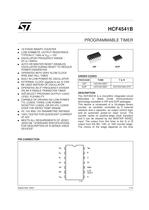
September 2002 1/10 n 16 STAGE BINARY COUNTER n LOW SYMMETR. OUTPUT RESISTANCE, TYPICALLY 100W at VDD = 15V n OSCILLATOR FREQUENCY RANGE : DC to 100KHz n AUTO OR MASTER RESET DISABLES OSCILLATOR DURING RESET TO REDUCE POWER DISSIPATION n OPERATES WITH VERY SLOW CLOCK RISE AND FALL TIMES n BUILT-IN LOW-POWER RC OSCILLATOR n EXTERNAL CLOCK (applied to pin 3) CAN BE USED INSTEAD OF OSCILLATOR n OPERATES AS 2n FREQUENCY DIVIDER OR AS A SINGLE-TRANSITION TIMER n Q/Q SELECT PROVIDES OUTPUT LOGIC LEVEL FLEXIBILITY n CAPABLE OF DRIVING SIX LOW POWER TTL LOADS, THREE LOW POWER SCHOTTKY LOADS, OR SIX HTL LOADS OVER THE RATED TEMP. RANGE n 5V, 10V AND 15V PARAMETRIC RATINGS n 100% TESTED FOR QUIESCENT CURRENT AT 20V n MEETS ALL REQUIREMENTS OF JEDEC JESD13B " STANDARD SPECIFICATIONS FOR DESCRIPTION OF B SERIES CMOS DEVICES" DESCRIPTION The HCF4541B is a monolithic integrated circuit fabricated in Metal Oxide Semiconductor technology available in DIP and SOP packages. This device is composed of a 16-stages binary counter, an oscillator controlled by 2 external resistors and a capacitor, an output control logic and an automatic power-on reset circuit. The counter varies on positive-edge clock transition and it can be cleared by the MASTER RESET input. The output from this timer is the Q or Q output from the 8th, 13th, or 16th counter stage. The choice of the stage depends on the time HCF4541B PROGRAMMABLE TIMER PIN CONNECTION ORDER CODES PACKAGE TUBE T & R DIP HCF4541BEY SOP HCF4541BM1 HCF4541M013TR DIP SOP
Abrir o catálogo na página 1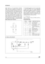
HCF4541B 2/10 select inputs A or B (see frequency selection table). The output is available in one of the two modes that can be selected via the MODE input pin 10 (see truth table). The output turns out as a continuos square wave, with a frequency equal to the oscillator frequency divided by 2N when this MODE input is a logic "1". When it is a logic "0" and after a MASTER RESET is started, and Q output has been selected, the output goes up to a high state after 2 N-1 counts. It remains in that state till another MASTER RESET pulse is apply or the mode input is a logic "1". The process...
Abrir o catálogo na página 2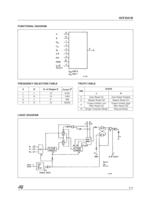
HCF4541B 3/10 FUNCTIONAL DIAGRAM FREQUENCY SELECTION TABLE TRUTH TABLE LOGIC DIAGRAM A B N. of Stages N Count 2N L L 13 8192 L H 10 1024 H L 8 256 H H 16 65536 PIN STATE L H 5 Auto Reset On Auto Reset Disable 6 Master Reset Off Master Reset On 9 Output Initially Low After Reset (Q) Output Initially High After Reset (Q) 10 Single Transition Mode Recycle Mode
Abrir o catálogo na página 3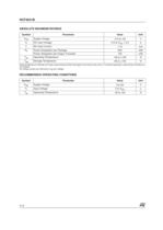
HCF4541B 4/10 ABSOLUTE MAXIMUM RATINGS Absolute Maximum Ratings are those values beyond which damage to the device may occur. Functional operation under these conditions is not implied. All voltage values are referred to VSS pin voltage. RECOMMENDED OPERATING CONDITIONS Symbol Parameter Value Unit VDD Supply Voltage -0.5 to +22 V VI DC Input Voltage -0.5 to VDD + 0.5 V II DC Input Current ± 10 mA PD Power Dissipation per Package 200 mW Power Dissipation per Output Transistor 100 mW Top Operating Temperature -55 to +125 °C Tstg Storage Temperature -65 to +150 °C Symbol Parameter Value Unit...
Abrir o catálogo na página 4
HCF4541B 6/10 DYNAMIC ELECTRICAL CHARACTERISTICS (Tamb = 25°C, CL = 50pF, RL = 200KW, tr = tf = 20 ns) (*) Typical temperature coefficient for all VDD value is 0.3 %/°C. DIGITAL TIMER APPLICATION A positive MASTER RESET pulse clears the counter and latch. The Output goes high and keeps up till the number of pulses, selected by A and B , are counted. This circuit is retriggerable and is as accurate as the input frequency. If a more accurate circuit is desired, an external clock can be used on pin 3. A set-up time equal to the width of the one shot output is required immediately following...
Abrir o catálogo na página 6
HCF4541B 7/10 TEST CIRCUIT CL = 50pF or equivalent (includes jig and probe capacitance) RL = 200KW RT = ZOUT of pulse generator (typically 50W)
Abrir o catálogo na página 7
HCF4541B 10/10 Information furnished is believed to be accurate and reliable. However, STMicroelectronics assumes no responsibility for the consequences of use of such information nor for any infringement of patents or other rights of third parties which may result from its use. No license is granted by implication or otherwise under any patent or patent rights of STMicroelectronics. Specifications mentioned in this publication are subject to change without notice. This publication supersedes and replaces all information previously supplied. STMicroelectronics products are not authorized...
Abrir o catálogo na página 10Todos os catálogos e folhetos técnicos STMicroelectronics
-
 STGW30NC60KD
14 Páginas
-
 STGB14NC60K STGD14NC60K
16 Páginas
-
 HD1750FX
8 Páginas
-
 TDA75610SLV
42 Páginas
-
 TDA7391
13 Páginas
-
 TDA7376B
15 Páginas
-
 TDA7375V
15 Páginas
-
 TDA2005
25 Páginas
-
 L4989D, L4989MD
19 Páginas
-
 L4938ED L4938EPD
20 Páginas
-
 L4949ED-E L4949EP-E
19 Páginas
-
 L4925
L492514 Páginas
-
 FDA903U
80 Páginas
-
 FDA803U
76 Páginas
-
 FDA903D
82 Páginas
-
 FDA803D
78 Páginas
-
 BALF-SPI2-02D3
13 Páginas
-
 LIS2DTW12
65 Páginas
-
 VL53L0X
40 Páginas
-
 LPS22HH
59 Páginas
-
 Standard products offer overview
13 Páginas
-
 M40SZ100W
20 Páginas
-
 A1C15S12M3
17 Páginas
-
 TSX923
32 Páginas
-
 TS1851
24 Páginas
-
 LMV321
17 Páginas
-
 TDA7303audio processor with loudness
20 Páginas
-
 Micro-sized Bluetooth® modules
4 Páginas
-
 Products and solutions for solar energy
28 Páginas
-
 SPC56 MCU family development tools
8 Páginas
-
 E-meter single-phase combo solution
4 Páginas
-
 Smart grid distribution and smart meters
20 Páginas
-
 Serial real-time clock (RTC) ICs
16 Páginas
-
 Advanced door electronics solutions
20 Páginas
-
 FFX: Full flexible amplification
7 Páginas
-
 TDA2003LG 10 W CAR AUDIO amplifier
8 Páginas
-
 TDA2003LG
8 Páginas
-
 L272 Dual Power Operational Amplifier
10 Páginas
-
 STA8058 GPS multi-chip module
14 Páginas
-
 TDA7410ND Signal Processor
34 Páginas
-
 TDA7410ND Signal Processor
34 Páginas
-
 TSA1204 DUAL CHANNEL
31 Páginas


Catálogos arquivados
-
 NEATSwitch
6 Páginas
-
 Power MOSFETs for metering
2 Páginas


