Excertos do catálogo

Data Sheet PS9031 2.5 A OUTPUT CURRENT, HIGH CMR, IGBT GATE DRIVE, 5-PIN SOP (LSO5 WITH 8mm CREEPAGE DISTANCE) PHOTOCOUPLER DESCRIPTION The PS9031 is an optically coupled isolator containing a GaAlAs LED on the input side and a photodiode, a signal processing circuit and power MOSFETs on the output side on one chip. Long creepage distance (8 mm MIN.) Large peak output current (2.5 A MAX., 2.0 A MIN.) High speed switching (tPLH tPHL = 175 ns MAX.) UVLO (Under Voltage Lock Out) protection with hysteresis High common mode transient immunity (CMH, CML = 50 kV/s MIN.) Operating Ambient Temperature (125 C MAX.) Embossed tape product : PS9031-F3 : 3000 pcs/reel Pb-Free product Safety standards UL approved: No. E72422 CSA approved: No. CA 101391 (CA5A, CAN/CSA-C22.2 60065, 60950) DIN EN 60747-5-5 (VDE 0884-5) approved (Option) APPLICATIONS IGBT, Power MOS FET Gate Driver Industrial inverter AC Servo Start of mass production Oct.2015 R08DS0131EJ0100
Abrir o catálogo na página 1
Chapter Title PACKAGE DIMENSIONS (UNIT: mm) PHOTOCOUPLER CONSTRUCTION Parameter Air Distance Outer Creepage Distance Isolation Distance
Abrir o catálogo na página 2
Chapter Title ORDERING INFORMATION Part Number Order Number Solder Plating Specification Packing Style Safety Standard Approval Pb-Free and Halogen Free (Ni/Pd/Au) Standard products (UL,CSA approved) 20 pcs (Tape 20 pcs cut) Embossed Tape 3 000 pcs/reel 20 pcs (Tape 20 pcs cut) Embossed Tape 3 000 pcs/reel UL,CSA approved DIN EN 60747-5-5 (VDE 0884-5): 2011-11 approved (Option) *1. For the application of the Safety Standard, following part number should be used. ABSOLUTE MAXIMUM RATINGS (TA = 25C, unless otherwise specified) Diode Parameter Forward Current Peak Transient Forward Current...
Abrir o catálogo na página 4
Chapter Title ELECTRICAL CHARACTERISTICS (at RECOMMENDED OPERATING CONDITIONS, VEE=GND, unless otherwise Specified) High Level Output Voltage Low Level Output Voltage High Level Supply Current Low Level Supply Current UVLO Threshold VOH VOL ICCH ICCL VUVLO+ VUVLO UVLOHYS Threshold Input Current (L H) IFLH VFHL UVLO Hysteresis Coupled Conditions IF = 10 mA, TA = 25C VR = 3 V, TA = 25C f = 1 MHz, VF = 0 V VO = (VCC 4 V) *2 VO = (VCC 15 V) *3 VO = (VEE + 2.5 V) *2 VO = (VEE + 15 V) *3 IO = 100 mA *4 IO = 100 mA VO = Open, IF = 10 mA VO = Open, VF = 0 to 0.8V VO > 5 V, IF = 10 mA...
Abrir o catálogo na página 5
Chapter Title TEST CIRCUIT Fig. 1 I OH Test Circuit Fig. 5 I CCH/ICCL Test Circuit Fig. 6 UVLO Test Circuit
Abrir o catálogo na página 6
Chapter Title Fig. 7 I FLH Test Circuit Fig. 8 t PLH, tPHL, tr, tf Test Circuit and Wave Forms VOUT tPLH Fig. 9 CMR Test Circuit and Wave Forms IF A 5
Abrir o catálogo na página 7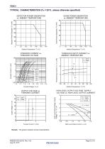
Chapter Title TYPICAL CHARACTERISTICS (TA = 25C, unless otherwise specified) DETECTOR POWER DISSIPATION vs. AMBIENT TEMPERATURE DIODE POWER DISSIPATION vs. AMBIENT TEMPERATURE 50 Diode Power Dissipation PD (mW) Detector Power Dissipation PC (mW) FORWARD CURRENT vs. FORWARD VOLTAGE THRESHOLD INPUT CURRENT vs. AMBIENT TEMPERATURE Threshold Input Current IFLH / IFHL (mA) OUTPUT VOLTAGE vs. FORWARD CURRENT HIGH LEVEL OUTPUT VOLTAGE SUPPLY VOLTAGE vs. HIGH LEVEL OUTPUT CURRENT 35 High Level Output Voltage Supply Voltage VOH VCC (V) High Level Output Current IOH (A) Remark The graphs indicate...
Abrir o catálogo na página 8
Chapter Title PROPAGATION DELAY TIME, PULSE WIDTH DISTORTION vs. FORWARD CURRENT LOW LEVEL OUTPUT VOLTAGE vs. LOW LEVEL OUTPUT CURRENT 175 VCC = 30 V, VEE = GND, IF = 0 mA Propagation Delay Time tPHL, tPLH (ns), Pulse Width Distortion (PWD) tPHL – tPLH (ns) Low Level Output Voltage VOL (V) PROPAGATION DELAY TIME, PULSE WIDTH DISTORTION vs. SUPPLY VOLTAGE Propagation Delay Time tPHL, tPLH (ns), Pulse Width Distortion (PWD) tPHL – tPLH (ns) Propagation Delay Time tPHL, tPLH (ns), Pulse Width Distortion (PWD) tPHL – tPLH (ns) PROPAGATION DELAY TIME, PULSE WIDTH DISTORTION vs. LOAD CAPACITANCE...
Abrir o catálogo na página 9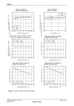
Chapter Title SUPPLY CURRENT vs. AMBIENT TEMPERATURE SUPPLY CURRENT vs. SUPPLY VOLTAGE 2.5 ICCH ICCL HIGH LEVEL OUTPUT VOLTAGE – SUPPLY VOLTAGE vs. AMBIENT TEMPERATURE High Level Supply Current ICCH (mA), Low Level Supply Current ICCL (mA) High Level Supply Current ICCH (mA), Low Level Supply Current ICCL (mA) Low Level Output Voltage VOL (V) LOW LEVEL OUTPUT VOLTAGE vs. AMBIENT TEMPERATURE LOW LEVEL OUTPUT CURRENT vs. AMBIENT TEMPERATURE HIGH LEVEL OUTPUT CURRENT vs. AMBIENT TEMPERATURE 3.0 Low Level Output Current IOL (A) 3.0 High Level Output Current IOH (A) 0.0 High Level Output Voltage...
Abrir o catálogo na página 10
Chapter Title OUTPUT VOLTAGE vs. SUPPLY VOLTAGE 14 Remark The graphs indicate nominal characteristics.
Abrir o catálogo na página 11
Chapter Title TAPING SPECIFICATIONS (UNIT: mm) Tape Direction Outline and Dimensions (Taps) Outline and Dimensions (Reel)
Abrir o catálogo na página 12
Chapter Title RECOMMENDED MOUNT PAD DIMENSIONS (UNIT: mm) Remark All dimensions in this figure must be evaluated before use.
Abrir o catálogo na página 13
Chapter Title NOTES ON HANDLING 1. Recommended soldering conditions (1) Infrared reflow soldering • Peak reflow temperature • Time of peak reflow temperature • Time of temperature higher than 220C • Time to preheat temperature from 120 to 180C • Number of reflows • Flux 260C or below (package surface temperature) 10 seconds or less 60 seconds or less 12030 s Three Rosin flux containing small amount of chlorine (The flux with a maximum chlorine content of 0.2 Wt% is recommended.) Package Surface Temperature T (°C) Recommended Temperature Profile of Infrared Reflow (2) Wave soldering •...
Abrir o catálogo na página 14
Chapter Title USAGE CAUTIONS 1. This product is weak for static electricity by designed with high-speed integrated circuit so protect against static electricity when handling. 2. Board designing (1) By-pass capacitor of more than 1.0 F is used between VCC and GND near device. Also, ensure that the distance between the leads of the photocoupler and capacitor is no more than 10 mm. (2) When designing the printed wiring board, ensure that the pattern of the IGBT collectors/emitters is not too close to the input block pattern of the photocoupler. If the pattern is too close to the input block...
Abrir o catálogo na página 15
Dependence of maximum safety ratings with package temperature Psi : total power dissipation
Abrir o catálogo na página 16Todos os catálogos e folhetos técnicos Renesas Electronics
-
 PowerMOSFET & IPD
8 Páginas
-
 RX FAMILY
68 Páginas
-
 Low Power SRAM
8 Páginas
-
 Renesas Microprocessor RZ Family Catalog
17 Páginas
-
 Renesas Capacitive Touch Solutions
7 Páginas
-
 Product Scout Automotive
8 Páginas
-
 R-IN32M3 Series
116 Páginas
-
 MCU Scout Industrial
82 Páginas
-
 RAA23014x RAA23015x
26 Páginas
-
 Industrial Communications
10 Páginas
-
 Remote I/O Tool Box
2 Páginas
-
 Cool Phoenix
2 Páginas
-
 Smart Solutions for Car Infotainment
5 Páginas
-
 RL78/G10 Datasheet
35 Páginas
-
 USB Solutions Product Guide
12 Páginas
-
 Selection Guide Low Power SRAM
8 Páginas
-
 Renesas General-Purpose Memory
31 Páginas


Catálogos arquivados
-
 RENESAS RL78 FAMILY MICROCONTROLLERS
44 Páginas
-
 Renesas Automotive
7 Páginas
-
 Renesas MPUs & MCUs RL78 Family
51 Páginas
-
 Body Control
5 Páginas
-
 Smart Solutions for a Smart Society
12 Páginas
-
 Smart Energy Solutions
8 Páginas
-
 Power supply system
13 Páginas
-
 Renesas Diodes General Presnetation
46 Páginas
-
 Renesas Memory General Presentation
67 Páginas
-
 Renesas Microcomputers General Presentation
801 Páginas
-
 Renesas MPU & MCU General Catalog
345 Páginas