
Excertos do catálogo
Intel® Core™ i7 Processor Family for LGA2011 Socket Datasheet – Volume 2 of 2 Supporting Desktop Intel® Core™ i7-4960X Extreme Edition Processor Series for the LGA2011 Socket Supporting Desktop Intel® Core™ i7-49xx and i7-48xx Processor Series for the LGA2011 Socket
Abrir o catálogo na página 1
INFORMATION IN THIS DOCUMENT IS PROVIDED IN CONNECTION WITH INTEL PRODUCTS. NO LICENSE, EXPRESS OR IMPLIED, BY ESTOPPEL OR OTHERWISE, TO ANY INTELLECTUAL PROPERTY RIGHTS IS GRANTED BY THIS DOCUMENT. EXCEPT AS PROVIDED IN INTEL'S TERMS AND CONDITIONS OF SALE FOR SUCH PRODUCTS, INTEL ASSUMES NO LIABILITY WHATSOEVER AND INTEL DISCLAIMS ANY EXPRESS OR IMPLIED WARRANTY, RELATING TO SALE AND/OR USE OF INTEL PRODUCTS INCLUDING LIABILITY OR WARRANTIES RELATING TO FITNESS FOR A PARTICULAR PURPOSE, MERCHANTABILITY, OR INFRINGEMENT OF ANY PATENT, COPYRIGHT OR OTHER INTELLECTUAL PROPERTY RIGHT. Legal...
Abrir o catálogo na página 2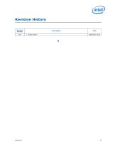
Revision History Revision Number 001 Initial release
Abrir o catálogo na página 13
(This page intentionally left blank)
Abrir o catálogo na página 14
Introduction This document is Volume 2 of 2 of the datasheet for the Intel® Core™ i7 processor family for LGA2011 Socket. Volume 2 provides register information for these processors. Volume 2 of 2 describes the Configuration Status Registers (CSRs) of each individual functional block in Uncore logic. The processor contains one or more PCI devices within each individual functional block. CSRs are the basic hardware elements that configure the Uncore logic to support various system topologies, memory configuration, and densities. The processor family contains one or more PCI devices within a...
Abrir o catálogo na página 15
Document Terminology Processor Terminology (Sheet 1 of 2) Terminology Third generation Double Data Rate SDRAM memory technology that is the successor to DDR2 SDRAM Direct Memory Access Direct Media Interface 2 Digital Thermal Sensor Enhanced Intel® SpeedStep® Technology Intel technology that allows the operating system to reduce power consumption when performance is not needed. The Execute Disable bit allows memory to be marked as executable or nonexecutable–when combined with a supporting operating system. If code attempts to run in non-executable memory the processor raises an error to...
Abrir o catálogo na página 16
Processor Terminology (Sheet 2 of 2) Terminology Power Control Unit Platform Environment Control Interface 64-bit, single-core or multi-core component (package) Processor Core The term “processor core” refers to silicon die itself which can contain multiple execution cores. Each execution core has an instruction cache, data cache, and 256KB L2 cache. All execution cores share the L3 cache. A unit of DRAM connecting four to eight devices in parallel. These devices are usually, but not always, mounted on a single side of a DDR3 DIMM. Processor interconnect between the different Uncore modules...
Abrir o catálogo na página 17
Related Documents Refer to the following documents for additional information. Processor Documents Document Document Number/ Location Intel® Core™ i7 Processor Family for the LGA2011 Socket Datasheet, Volume 1 Desktop Intel Core™ i7 Processor Family for the LGA2011 Thermal Mechanical Specification and Design Guide Intel® Core™ i7 Processor Family for the LGA2011 Socket Specification Update Intel® X79 Express Chipset Datasheet Intel® X79 Express Chipset Thermal Mechanical Specifications and Design Guide Advanced Configuration and Power Interface Specification 3.0 http://www.pcisig.com/...
Abrir o catálogo na página 18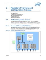
Registers Overview and Configuration Process Registers Overview and Configuration Process This chapter covers • • • • Platform Configuration Structure Configuration Register Rules Register Terminology Notational Conventions Platform Configuration Structure The DMI2 physically connects the processor and the PCH. From a configuration standpoint the DMI2 is a logical extension of PCI Bus 0. DMI2 and the internal devices in the processor IIO and PCH logically constitute PCI Bus 0 to configuration software. As a result, all devices internal to the processor and the PCH appear to be on PCI Bus 0....
Abrir o catálogo na página 19
Registers Overview and Configuration Process • Device 0: DMI2 Root Port. Logically this appears as a PCI device residing on PCI Bus 0. Device 0 contains the standard PCI header registers, extended PCI configuration registers and DMI2 device specific configuration registers. • Device 1: PCI Express* Root Port 1a, 1b. Logically this appears as a “virtual” PCI-to-PCI bridge residing on PCI Bus 0 and is compliant with PCI Express* Local Bus Specification Revision 2.0. Device 1 contains the standard PCI Express*/PCI configuration registers including PCI Express* Memory Address Mapping registers....
Abrir o catálogo na página 20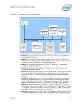
Registers Overview and Configuration Process Processor Uncore Devices Map Bus = CPUBUSNO (1)* Power Control Unit (PCU) (Device 10, Function 0‐ 4) Integrated Memory Controller (Device 15 General Registers, TAD Rank and Timings, Device 16 Thermal Control and Test Registers) Performance Monitoring (Device 14,16,19) • Device 10: Processor Power Control Unit. Device 10, Function 0-4 contains the configurable PCU registers. • Device 11: Processor Interrupt Event Handling (UBox). Device 11, Function 0 contains the processor Interrupt Control Registers. Device 11, Function 3 contains the...
Abrir o catálogo na página 21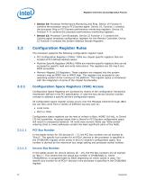
Registers Overview and Configuration Process • Device 19: Processor Performance Monitoring and Ring. Device 19 Function 0 contains the processor ring to PCI Express agent. Device 19, Function 1 contains the processor Ring to PCI Express performance monitoring registers. Device 19, Function 4 -6 contains the processor performance monitoring registers. • Device 22: Processor Core Broadcast. Device 22 Function 1-2 contains the Caching agent broadcast configuration registers for the Memory Controller. Device 22 Function 0 contains the System Address Decode Registers. Configuration Register...
Abrir o catálogo na página 22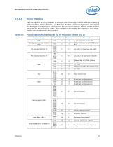
Registers Overview and Configuration Process Device Mapping Each component in the processor is uniquely identified by a PCI bus address consisting of Bus Number, Device Number, and Function Number. Device configuration is based on the PCI Type 0 configuration conventions. All processor registers appear on the PCI bus assigned for the processor socket. Bus number is derived by the maximum bus range setting and processor socket number. Functions Specifically Handled by the Processor (Sheet 1 of 2) Register Group x4 Link from Processor to PCH Device 0 will work as a x4 PCI Express Port PCI...
Abrir o catálogo na página 23Todos os catálogos e folhetos técnicos Intel
-
 10th Gen Intel® Core
7 Páginas
-
 10th Gen
8 Páginas
-
 nuc-celeron
4 Páginas
-
 Intel® Optane™ SSD DC P4800X Series
2 Páginas
-
 Intel® NUC 8 Home Mini PC
4 Páginas
-
 Intel® Xeon® Scalable Platform
14 Páginas
-
 Intel® Ethernet Controller XL710
1726 Páginas
-
 Intel® Xeon® Processor E3-1200 v5
130 Páginas
-
 Intel® Quark™ SoC X1000 Series
934 Páginas
-
 Intel® X99 Chipset
4 Páginas
-
 Mini PC - Intel® NUC Kit DC3217IYE
4 Páginas
-
 Mini PC?Intel® NUC Kit NUC5i5RYH
4 Páginas
-
 Intel® Desktop Board DQ67EP
4 Páginas
-
 Intel® Ethernet Switch FM4000
270 Páginas
-
 Intel® NUC Board DE3815TYBE
82 Páginas
-
 S2600GZ and S2600GL
245 Páginas
-
 Intel® Solid-State Drive DC P3700 Series
42 Páginas
-
 i7-lga2011
314 Páginas
-
 c600-series
936 Páginas
-
 b75-express
4 Páginas
-
 desktop-board
4 Páginas
-
 3rd-gen-core-desktops
2 Páginas
-
 /3rd-gen-core
2 Páginas


Catálogos arquivados
-
 Intel® Server System SR2600UR
8 Páginas
-
 Intel® Ethernet Controllers
2 Páginas
-
 Intel® 3450 Chipset
2 Páginas
-
 Intel® 3000 and 3010 Chipset
4 Páginas
-
 Intel® X58 Express Chipset
4 Páginas
-
 Intel® Server Board S1200BT
8 Páginas
-
 Intel® Desktop Board DX58SO2
4 Páginas
-
 Intel® Xeon® Processor 5000 Series Datasheet
104 Páginas
-
 Intel® I/O Processor Overview
4 Páginas


