ATA664251 16K Flash Microcontroller with LIN Transceiver, 5V Regulator, Watchdog, 8-channel High Voltage Switch / LED Interface with High Voltage Current Sources, 16-bit SPI
1 /
290Páginas

Excertos do catálogo
ATA664251 16K Flash Microcontroller with LIN Transceiver, 5V Regulator, Watchdog, 8-channel High-voltage Switch Interface with High-voltage Current Sources, 16-bit SPI DATASHEET General Features ● Single-package high performance, low-power AVR® 8-bit microcontroller with LIN transceiver, 5V regulator (80mA current capability), watchdog, 8-channel high-voltage (HV) switch interface with high-voltage (HV) current sources and 16-bit serial programming interface (SPI) ● Very low current consumption in sleep mode ● 16-Kbyte flash memory for application program ● Supply voltage up to 40V ● Operating voltage: 5V to 27V ● Temperature range: Tcase = –40°C to +125°C ● QFN48, 7mm × 7mm package
Abrir o catálogo na página 1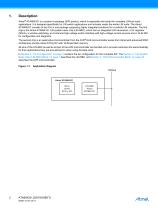
Description Atmel® ATA664251 is a system-in-package (SiP) product, which is especially well suited for complete LIN-bus node applications. It is designed specifically for LIN switch applications and includes nearly the entire LIN node. The Atmel ATA664251 consists of two ICs in one package supporting highly integrated solutions for in-vehicle LIN networks. The first chip is the Atmel ATA664151 LIN system basis chip (LIN-SBC), which has an integrated LIN transceiver, a 5V regulator (80mA), a window watchdog, an 8-channel high-voltage switch interface with high-voltage current sources and a...
Abrir o catálogo na página 2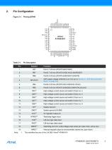
GND VCC NTRIG TXD RXD NRES NIRQ MISO MOSI SCK NCS PWM1 High-voltage current source and switch I/O-pin no. 4 High-voltage current source and switch I/O-pin no. 5 High-voltage current source and switch I/O-pin no. 6 High-voltage current source and switch I/O-pin no. 7 High-voltage current source and switch I/O-pin no. 8 AVR supply voltage (referred to as VCC pin in Section 5. “AVR Microcontroller Block” on page 45) System ground LIN-SBC Watchdog trigger input LIN-bus logic data input LIN-bus logic data output Watchdog and VCC undervoltage reset output pin (open drain, active low) Interrupt...
Abrir o catálogo na página 3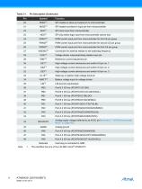
SPI master-in-slave-out output pin to microcontroller SPI master-out-slave-in input pin from microcontroller SPI clock input from microcontroller SPI chip select logic input from microcontroller (active low) PWM control input port from microcontroller for first CS pin group PWM control input port from microcontroller for second CS pin group PWM control input port from microcontroller for third CS pin group Voltage divider output/watchdog disable input pin Reference current adjustment pin High-voltage current sink/source and switch I/O-pin no. 1 High-voltage current sink/source and switch...
Abrir o catálogo na página 4
Absolute Maximum Ratings Stresses beyond those listed under “Absolute Maximum Ratings” may cause permanent damage to the device. This is a stress rating only and functional operation of the device at these or any other conditions beyond those indicated in the operational sections of this specification is not implied. Exposure to absolute maximum rating conditions for extended periods may affect device reliability. Parameters ESD according to IBEE LIN EMC Test Spec. 1.0 following IEC 61000-4-2 - Pin VS, LIN to GND - Pin CL15 (10kΩ, 47nF) to GND - Pin VBATT (10nF) to GND - Pins CSx (10nF) to...
Abrir o catálogo na página 5
Maximum Ratings of the LIN-SBC (Continued) Stresses beyond those listed under “Absolute Maximum Ratings” may cause permanent damage to the device. This is a stress rating only and functional operation of the device at these or any other conditions beyond those indicated in the operational sections of this specification is not implied. Exposure to absolute maximum rating conditions for extended periods may affect device reliability. Parameters Voltage Levels on pins1) - LIN - VBATT (with 51Ω/10nF) -> DC voltage Voltage levels on logic/low-voltage pins: RXD, TXD, NRES, NTRIG, WDOSC, PWMy,...
Abrir o catálogo na página 6
LIN System Basis Chip (LIN-SBC) Block 8-channel HV switch interface with HV current sources Linear low-drop voltage regulator, up to 80mA current capability, VCC = 5.0V ±2% Fulfills the OEM “Hardware Requirements for LIN in Automotive Applications Rev.1.3” LIN master and slave operation possible Supply voltage up to 40V Operating voltage VS = 5V to 27V Internal voltage divider for VBattery sensing (±2%) 16-bit serial interface (daisy-chain-capable) for configuration and diagnosis Typically 8µA supply current during sleep mode Typically 35µA supply current in active low-power mode VCC...
Abrir o catálogo na página 7
Description The LIN-SBC includes an eight-channel high voltage switch interface, a LIN 2.1 and SAEJ2602-2-compliant LIN transceiver, low-drop voltage regulator, and an adjustable Window Watchdog. The voltage regulator has an output voltage of 5V and is able to drive 80mA. This chip combination is especially designed for LIN switch applications. It is designed to handle low data-rate communication in vehicles (such as in convenience electronics). Improved slope control at the LIN driver ensures secure data communication up to 20kBaud. Sleep Mode and Active Low-power Mode guarantee minimal...
Abrir o catálogo na página 8
Physical Layer Compatibility Since the LIN physical layer is independent of higher LIN layers (such as the LIN protocol layer), all nodes with a LIN physical layer as per release version 2.1 can be mixed with LIN physical layer nodes found in older versions (i.e., LIN 1.0, LIN 1.1, LIN 1.2, LIN 1.3, LIN 2.0), without any restrictions. Supply Pin (VS) The operating voltage is VS = 5V to 27V. An undervoltage detection is implemented to disable data transmission via the LIN bus and the switch interface if VVS falls below VVSth in order to avoid false bus messages. After switching on VS, the IC...
Abrir o catálogo na página 9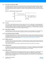
Bus Logic Level Output Pin (RXD) This output pin reports the state of the LIN bus to the microcontroller. LIN high (recessive state) is reported by a high level, LIN low (dominant state) is reported by a low level at RXD. The output has push-pull characteristics meaning no external time defining measures are required. During states of disabled LIN-PHY (configuration bit “LINE” = 0), pin RXD is at high level. Please note that the signal on the RXD pin is not valid for a certain period of time upon activation of the LIN transceiver (tRXDinvalid). Figure 4-2. RXD Timing upon Transceiver Enable...
Abrir o catálogo na página 10Todos os catálogos e folhetos técnicos Atmel
-
 32-bit Microcontrollers
20 Páginas
-
 MCUs Driving Displays
12 Páginas
-
 Touch and 3D Gesture Control
12 Páginas
-
 16-bit MCUs and DSCs
20 Páginas
-
 XLP PIC® MCUs
8 Páginas
-
 8-bit MCUs
16 Páginas
-
 ATA663201/ATA663203/ATA663231/ATA663254
29 Páginas
-
 AT93C56B/66B Automotive
17 Páginas
-
 Atmel AT86RF215 Device Family
235 Páginas
-
 AT24C01C/02C
22 Páginas
-
 Product Selection Guide - serial EEPROM
24 Páginas
-
 maXTouch U Series - Flyer
2 Páginas
-
 ATA2536T Low-voltage IR Receiver ASSP
14 Páginas
-
 AT42QT1040 4-channel QTouch® Sensor IC
22 Páginas


Catálogos arquivados
-
 tinyAVR ATtiny24/44/84 Preliminary
240 Páginas
-
 Smart Battery AVR ATmega406 Preliminary
263 Páginas
-
 ATmega164P/324P/644P Preliminary
440 Páginas
-
 ATmega48P/88P/168P/328P Preliminary
426 Páginas
-
 ATmega1284P Preliminary
356 Páginas
-
 AT90PWM216/316
359 Páginas
-
 AT90PWM2, AT90PWM3, AT90PWM2B, AT90PWM3B
361 Páginas
-
 ATmega329/3290/649/6490 Preliminary
392 Páginas
-
 ATmega329P/3290P Preliminary
388 Páginas
-
 AT90CAN32/64/128
428 Páginas
-
 ATmega640/1280/1281/2560/2561 Preliminary
448 Páginas
-
 AT86RF230 Preliminary
98 Páginas
-
 ATmega48/88/168 Automotive
335 Páginas
-
 ATtiny25, ATtiny45, ATtiny85 Automotive
192 Páginas
-
 ATtiny24/44/84 Automotive Preliminary
225 Páginas
-
 AT86RF231 Preliminary
180 Páginas
-
 Atmel Product Selection Guide - Jan 2008
11 Páginas
-
 Biometrics (Fingerprint Sensor)
20 Páginas
