LTC3838-1 - Dual, Fast, Accurate Step-Down DC/DC Controller with Dual Differential Output Sensing
1 /
52Páginas

Excertos do catálogo
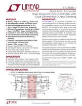
LTC3838-1 Dual, Fast, Accurate Step-Down DC/DC Controller with Dual Differential Output Sensing DESCRIPTION FEATURES Wide VIN Range: 4.5V to 38V, VOUT: 0.6V to 5.5V n Two Independent Channels: Dual/Single Output n Output Voltage Regulation Accuracy: ±0.67% (VOUT1) and ±0.75% (VOUT2) Over Temperature n Differential Remote Output Sensing: Up to ±500mV (VOUT1) and ±200mV (VOUT2) Ground Deviations n Controlled On-Time, Valley Current Mode Control n Fast Load Transient Response Without Clock Delay n Detect Transient Release (DTR) Reduces V OUT Overshoot n Frequency Programmable from 200kHz to 2MHz, Synchronizable to External Clock n t ON(MIN) = 30ns, tOFF(MIN) = 90ns n R SENSE or Inductor DCR Current Sensing n Overvoltage Protection and Current Limit Foldback n Power Good Output Voltage Monitor n Output Voltage Tracking and Adjustable Soft Start-Up n Thermally Enhanced 38-Pin (5mm × 7mm) QFN Package n APPLICATIONS n n n Distributed Power Systems; Power Supply for ASIC Computing, Data Storage, Communication Systems Low Voltage, High Current, and/or High Step-Down Ratio Converters That Demand Tight Load Transient Regulation The LTC®3838-1 is a dual-channel, PolyPhase® synchronous step-down DC/DC switching regulator controller. Two independent channels drive all N-channel power MOSFETs. The controlled on-time, valley current mode control architecture allows for not only fast response to transients without clock delay, but also constant frequency switching at steady load condition. Its proprietary loadrelease transient detection feature (DTR) significantly reduces overshoot at low output voltages. A precision internal reference enables accurate differential output regulation. The dual channels can either provide two independent output voltages, or be combined into multiphase single-output configuration. The switching frequency can be programmed from 200kHz to 2MHz with an external resistor and can be synchronized to an external clock. Very low tON and tOFF times allow for near 0% and near 100% duty cycles, respectively. Voltage tracking soft start-up and multiple safety features are provided. See Table 1 for a comparison of LTC3838, LTC3838-1 and LTC3838-2. L, LT, LTC, LTM, PolyPhase, OPTI-LOOP, Linear Technology and the Linear logo are registered trademarks and Hot Swap is a trademark of Linear Technology Corporation. All other trademarks are the property of their respective owners. Protected by U.S. Patents, including 5481178, 5847554, 6580258, 6304066, 6476589, 6774611. TYPICAL APPLICATION 1.2V/1.5V, 15A, 350kHz Step-Down Converter (Refer to Figure 16 for Complete Design) Efficiency/Power Loss VIN 4.5V TO 38V SENSE1– SENSE1+ SENSE2+ LTC3838-1 SW2 BOOST1 330µF ×2 + 10k DRVCC1 0.1µF 4.7µF 10k 0.56µH DRVCC2 VOUT2 1.5V 15A BOOST2 BG1 0.1µF BG2 PGND 10k/ 10k 15k EXTVCC VOUTSENSE1+ VOUTSENSE1– 15k + 330µF ×2 VDFB2+ ITH1 RT SGND VRNG RUN1 ITH2 2.0 80 1.5 EFFICIENCY 70 POWER LOSS 60 1.0 0.5 50 40 VDFB2– TRACK/SS1 TRACK/SS2 115k EFFICIENCY (%) TG2 SW1 0.56µH 90 INTVCC TG1 2.5 FORCED CONTINUOUS MODE DISCONTINUOUS MODE POWER LOSS (W) VIN VOUT1 1.2V 15A 100 SENSE2– VIN = 12V VOUT = 1.2V 0.1 1 LOAD CURRENT (A) 10 0 38381 TA01b MODE_PLLIN CLKOUT PHASMD RUN2 38381 TA01a For more information www.linear.com3838-1 38381f 1
Abrir o catálogo na página 1
ABSOLUTE mnximum Rnnnos INTVcc, DRVcci, DRVCC2, EXTVCC, PG00D1, Operating Junction Temperature Range (PIN 39) IS PGND, MUST BE SOLDERED TO PCB ORD€R inFORffMTIOn Consult LTC Marketing for parts specified with wider operating temperature ranges. *The temperature grade is identified by a label on the shipping container. Consult LTC Marketing for information on non-standard lead based finish parts. For more information on lead free part marking, go to: http://www.linear.com/leadfree/ For more information on tape and reel specifications, go to: http://www.linear.com/tapeandreel/ Table 1....
Abrir o catálogo na página 2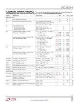
The • denotes the specifications which apply junction temperature range, otherwise specifications are at TA = 25°C. Vm = 15V unless otherwise noted over the specified operating Main Control Loops Current Sensing ^^^J TECHNOLOGY
Abrir o catálogo na página 3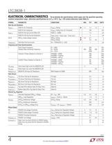
€l€CTMCm CHRRnCTCRISTICS junction temperature range, otherwise specifications are The • denotes the specifications which apply over the specified operating at TA = 25°C. V|N = 15V unless otherwise noted (Note 3). Frequency and Clock Synchronization Gate Drivers PGood Output ^^^J TECHNOLOGY
Abrir o catálogo na página 4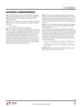
LTC3838-1 ELECTRICAL CHARACTERISTICS Note 1: Stresses beyond those listed under Absolute Maximum Ratings may cause permanent damage to the device. Exposure to any Absolute Maximum Rating condition for extended periods may affect device reliability and lifetime. Note 2: The junction temperature (TJ, in °C) is calculated from the ambient temperature (TA, in °C) and power dissipation (PD, in Watts) according to the formula: TJ = TA + (PD • θJA) where θJA (in °C/W) is the package thermal impedance. Note 3: The LTC3838-1 is tested under pulsed load conditions such that TJ ≈ TA. The LTC3838E-1 is...
Abrir o catálogo na página 5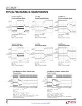
TVPICRL p€RFORmnnc€ CHnnncTCMSTics Transient Response (Forced Continuous Mode) Load Step (Forced Continuous Mode) Load Release (Forced Continuous Mode) FIGURE 17 CIRCUIT CHANNEL 1 FIGURE 17 CIRCUIT CHANNEL 1 FIGURE 17 CIRCUIT CHANNEL 1 Transient Response (Discontinuous Mode) Load Step (Discontinuous Mode) FIGURE 17 CIRCUIT CHANNEL 1 Load Release (Discontinuous Mode) FIGURE 17 CIRCUIT CHANNEL 1 FIGURE 17 CIRCUIT CHANNEL 1 Load Release with Detect Transient (DTR) Feature Enabled Load Release with Detect Transient (DTR) Feature Disabled FIGURE 17 CIRCUIT CHANNEL 1 MODIFIED: FROM DTR1 PIN:...
Abrir o catálogo na página 6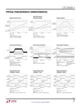
TVPICRL p€RFORmnnc€ CHnnncTCMSTics Regular Soft Start-Up Soft Start-Up Into Prebiased Output Output Tracking FORCED CONTINUOUS MODE FIGURE 17 CIRCUIT CHANNEL 1 FIGURE 17 CIRCUIT CHANNEL 1 FORCED CONTINUOUS MODE FIGURE 17 CIRCUIT CHANNEL 1 Overcurrent Protection Short-Circuit Protection Overvoltage Protection 'FULL CURRENT LIMIT ' THAN HALF OF REGULATED FORCED CONTINUOUS MODE FIGURE 17 CIRCUIT CHANNEL 1 FIGURE 17 CIRCUIT CHANNEL 1 OVERVOLTAGE CREATED BY APPLYING FORCED CONTINUOUS VOUT IS PULLED MODE BELOW OVERVOLTAGE FIGURE 17 CIRCUIT CHANNEL 1 Phase Relationship: MODE/PLLIN = 333kHz...
Abrir o catálogo na página 7Todos os catálogos e folhetos técnicos ADI
-
 LTC2068
30 Páginas
-
 LTC6373
34 Páginas
-
 ADL9006
16 Páginas
-
 ADL8104
23 Páginas
-
 AD4115
52 Páginas
-
 ADUM7702
22 Páginas
-
 AD7383
33 Páginas
-
 AD7384
33 Páginas
-
 AD4114
49 Páginas
-
 ADUM7704
22 Páginas
-
 AD7134
86 Páginas
-
 LTspice IV
53 Páginas
-
 New Products Catalog
43 Páginas
-
 RF/IF Amplifiers
9 Páginas
-
 SAR ADC Drivers
2 Páginas
-
 Products for Harsh Environments
4 Páginas
-
 SmartMesh Brochure
8 Páginas
-
 INDUSTRIAL SIGNAL CHAIN
24 Páginas
-
 AUTOMOTIVE ELECTRONIC SOLUTIONS
48 Páginas
-
 µModule® Power Product Family
7 Páginas
-
 Battery Management Solutions
32 Páginas
-
 High Performance DC/DC Controllers
20 Páginas
-
 DC/DC uModule Power Products
32 Páginas
-
 Wireless & RF Solution
36 Páginas
-
 LT2940 - Power and Current Monitor
24 Páginas
-
 LT6656 - 1
18 Páginas
-
 LT3596 - 60V Step-Down LED Driver
22 Páginas


Catálogos arquivados
-
 Automotive & Transportation Solutions
56 Páginas
-
 New Products Catalog
39 Páginas
-
 High Performance DC/DC Controllers
21 Páginas
-
 Power Management for Portable Products
32 Páginas
-
 Power Management for LEDs
24 Páginas
-
 High Speed ADC Products Brochure
14 Páginas