LTC3114-1 - 40V, 1A Synchronous Buck-Boost DC/DC Converter with Programmable Output Current
1 /
32Páginas

Excertos do catálogo
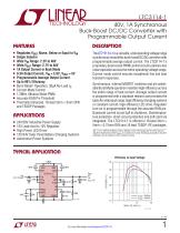
Buck-Boost DC/DC Converter with Programmable Output Current ■ Regulates VQUT Above, Below or Equal to ViN ■ Wide VQUT Range: 2.7V to 40V ■ 1A Output Current in Buck Mode ■ Programmable Average Output Current ■ Burst Mode® Operation, 30uA No-Load lQ ■ Current Mode Control ■ 24V/28V Industrial Power Supply ■ High Power LED Driver ■ 12V/24V Solar Panel Battery Charging Systems ■ Automotive Power Systems The LTC®3114-1 is a versatile, wide operating voltage range synchronous monolithic buck-boost DC/DC converterwith programmable average output current. The LTC3114-1 's proprietary buck-boost PWM control circuitry delivers low noise operation across the entire operating voltage range. Current mode control ensures exceptional line and load transient responses. Synchronous, internal MOSFET switches and pin select- able Burst Mode operation maintain high efficiency across the entire range of load current. Average output current is programmed with a standard resistor and provides the basisforwide input range, high efficiency charging systems or constant current, high efficiency LED drive. Regulator turn-on is programmable through the accurate RUN pin. Quiescent current is just 3uA in shutdown. Overtempera- ture protection, short-circuit protection and soft-start are 5mm x 0.75mm DFN and 16 lead TSSOP (FE) packages. XT, LT, LTC, LTM, Burst Mode, LTspice, uModule, Linear Technology and the Linear logo are registered trademarks and No RSENSE is a trademark of Linear Technology Corporation. All other trademarks are the property of their respective owners. TVPicni nppucnTion .^.IOUFI- PV|N Efficiency vs Input Voltage TECHNOLOGY For more information www.linear.com/LTC3114-1
Abrir o catálogo na página 1
LTC3114-1 ABSOLUTE MAXIMUM RATINGS DHC PACKAGE 16-LEAD (5mm × 3mm) PLASTIC DFN TJMAX = 150°C, θJA = 43°C/W (4-LAYER BOARD), θJC = 4°C/W EXPOSED PAD (PIN 17) IS PGND, MUST BE SOLDERED TO PCB FOR RATED THERMAL PERFORMANCE FE PACKAGE 16-LEAD PLASTIC TSSOP TJMAX = 150°C, θJA = 38°C/W EXPOSED PAD (PIN 17) IS PGND, MUST BE SOLDERED TO PCB FOR RATED THERMAL PERFORMANCE ORDER INFORMATION LEAD FREE FINISH PART MARKING* PACKAGE DESCRIPTION TEMPERATURE RANGE Consult LTC Marketing for parts specified with wider operating temperature ranges. *The temperature grade is identified by a label on the...
Abrir o catálogo na página 2
The l denotes the specifications which apply over the specified operating junction temperature range, otherwise specifications are at TA = 25°C (Note 2). VIN = 24V, VOUT = 5V, unless otherwise noted. PARAMETER Output Operating Voltage Undervoltage Lockout Threshold on LDO VLDO Rising VIN Quiescent Current in Shutdown VIN Quiescent Current in Burst Mode Operation Oscillator Frequency Oscillator Frequency Variation Feedback Voltage Feedback Voltage Line Regulation Error Amplifier Transconductance PROG Current Gain Switch D Current = 1A Switch D Current = 500mA Switch D Current = 100mA (Note...
Abrir o catálogo na página 3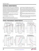
LTC3114-1 ELECTRICAL CHARACTERISTICS operating junction temperature range. The LTC3114H-1 specifications are guaranteed over the –40°C to 150°C operating junction temperature range. The LTC3114MP-1 specifications are guaranteed over the –55°C to 150°C operating junction temperature range. High junction temperatures degrade operating lifetime; operating lifetime is derated for junction temperatures greater than 125°C. The maximum ambient temperature consistent with these specifications is determined by specific operating conditions in conjunction with board layout, the rated package thermal...
Abrir o catálogo na página 4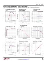
LTC3114-1 TYPICAL PERFORMANCE CHARACTERISTICS (TA = 25°C unless otherwise specified) 170 Burst Mode Operation Threshold vs VIN No-Load Input Current vs VIN, PWM Mode LOAD INCREASING LOAD DECREASING VOUT = 5V VOUT = 12V 10 INPUT VOLTAGE (V) VIN = 12V RPROG = 64.7k 10 OUTPUT VOLTAGE (V) Combined LDO, PLDO Supply Current vs VIN Combined LDO, PLDO Supply Current vs LDO 8.50 COMBINED LDO, PLDO CURRENT (mA) 8.00 COMBINED LDO, PLDO CURRENT (mA) CHANGE IN VOUT NORMALIZED TO VIN = 2.7V (%) Output Voltage Line Regulation Output Voltage Load Regulation PROG Regulation Voltage vs Temperature Average...
Abrir o catálogo na página 5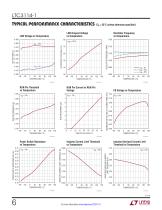
LTC3114-1 TYPICAL PERFORMANCE CHARACTERISTICS (TA = 25°C unless otherwise specified) LDO Dropout Voltage vs Temperature Inductor Overload Current Limit Threshold vs Temperature 2.70 INDUCTOR OVERLOAD CURRENT LIMIT THRESHOLD (A) INDUCTOR CURRENT LIMIT THRESHOLD (A) POWER SWITCH RESISTANCE A/D (Ω) Inductor Current Limit Threshold vs Temperature Power Switch Resistance vs Temperature 0.39 NORMAIZED FB VOLTAGE (% CHANGE FROM 25°C) Oscillator Frequency vs Temperature
Abrir o catálogo na página 6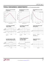
LTC3114-1 TYPICAL PERFORMANCE CHARACTERISTICS (TA = 25°C unless otherwise specified) 115 SW1/SW2 Minimum Low Times vs Temperature 120 INDUCTOR ZERO CURRENT THRESHOLD (mA) Inductor Zero Current Threshold vs Temperature Load Transient in Buck Mode, 100mA to 600mA LOAD CURRENT 500mA/DIV Output Voltage Ripple in Burst Mode Operation VIN = 14V 200µs/DIV LOAD = 10mA FRONT PAGE CIRCUIT 5V Output Voltage Response to Fast Line Transient (4V to 28V in 10µs) Output Voltage Ripple in PWM Mode Burst Mode Operation to PWM Mode Output Voltage Response LOAD CURRENT 500mA/DIV Load Transient in Boost Mode,...
Abrir o catálogo na página 7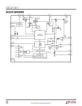
LTC3114-1 BLOCK DIAGRAM PVIN INDUCTOR ISENSE OUTPUT CURRENT SENSE 1.2MHz OSCILLATOR SOFT-START 1V BIAS GENERATOR BANDGAP REFERENCE POR OVERTEMPERATURE PROTECTION
Abrir o catálogo na página 8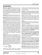
LTC3114-1 PIN FUNCTIONS PGND (Pin 1, Exposed Pad Pin 17): Power Ground Connections. The PGND pin must be electrically connected to a power ground plane in the application. The exposed pad is an additional power ground connection in parallel with Pin 1. Optimal thermal performance requires that the exposed pad be soldered to the PC board and preferably to a ground plane. functions. Refer to the Applications Information section for complete details on how to select the proper values for RPROG and CPROG. SW2 (Pin 2): Buck-Boost Converter Power Switch Pin. This pin is connected to one side of...
Abrir o catálogo na página 9Todos os catálogos e folhetos técnicos ADI
-
 LTC2068
30 Páginas
-
 LTC6373
34 Páginas
-
 ADL9006
16 Páginas
-
 ADL8104
23 Páginas
-
 AD4115
52 Páginas
-
 ADUM7702
22 Páginas
-
 AD7383
33 Páginas
-
 AD7384
33 Páginas
-
 AD4114
49 Páginas
-
 ADUM7704
22 Páginas
-
 AD7134
86 Páginas
-
 LTspice IV
53 Páginas
-
 New Products Catalog
43 Páginas
-
 RF/IF Amplifiers
9 Páginas
-
 SAR ADC Drivers
2 Páginas
-
 Products for Harsh Environments
4 Páginas
-
 SmartMesh Brochure
8 Páginas
-
 INDUSTRIAL SIGNAL CHAIN
24 Páginas
-
 AUTOMOTIVE ELECTRONIC SOLUTIONS
48 Páginas
-
 µModule® Power Product Family
7 Páginas
-
 Battery Management Solutions
32 Páginas
-
 High Performance DC/DC Controllers
20 Páginas
-
 DC/DC uModule Power Products
32 Páginas
-
 Wireless & RF Solution
36 Páginas
-
 LT2940 - Power and Current Monitor
24 Páginas
-
 LT6656 - 1
18 Páginas
-
 LT3596 - 60V Step-Down LED Driver
22 Páginas


Catálogos arquivados
-
 Automotive & Transportation Solutions
56 Páginas
-
 New Products Catalog
39 Páginas
-
 High Performance DC/DC Controllers
21 Páginas
-
 Power Management for Portable Products
32 Páginas
-
 Power Management for LEDs
24 Páginas
-
 High Speed ADC Products Brochure
14 Páginas