LTC2368-24 - 24-Bit, 1Msps, Pseudo- Differential Unipolar SAR ADC with Integrated Digital Filter
1 /
30Páginas

Excertos do catálogo
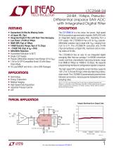
LTC2368-24 24-Bit, 1Msps, PseudoDifferential Unipolar SAR ADC with Integrated Digital Filter DESCRIPTION Guaranteed 24-Bits No Missing Codes nn ±0.5ppm INL (Typ) nn Integrated Digital Filter with Real-Time Averaging nn Low Power: 21mW at 1Msps nn 98dB SNR (Typ) at 1Msps nn 140dB Dynamic Range (Typ) at 15.25sps nn –116dB THD (Typ) at f = 2kHz IN nn 50Hz/60Hz Rejection nn Guaranteed Operation to 85°C nn Single 2.5V Supply nn Pseudo-Differential Unipolar Input Range: 0V to V REF nn 1.8V to 5V SPI-Compatible Serial I/O with DaisyChain Mode nn 16-Lead MSOP and 4mm × 3mm DFN Packages The LTC®2368-24 is a low noise, low power, high speed 24-bit successive approximation register (SAR) ADC with an integrated digital averaging filter. Operating from a 2.5V supply, the LTC2368-24 has a 0V to VREF pseudodifferential unipolar input range with VREF ranging from 2.5V to 5.1V. The LTC2368-24 consumes only 21mW (Typ) and achieves ±4.5ppm INL maximum and no missing codes at 24 bits. The LTC2368-24 has an easy to use integrated digital averaging filter that can average 1 to 65536 conversion results real-time, dramatically improving dynamic range from 98dB at 1Msps to 140dB at 15.25sps. No separate programming interface or configuration register is required. The high speed SPI-compatible serial interface supports 1.8V, 2.5V, 3.3V and 5V logic while also featuring a daisychain mode. The LTC2368-24 automatically powers down between conversions, reducing power dissipation at lower sampling rates. APPLICATIONS Seismology Energy Exploration nn Medical Imaging nn High Speed Data Acquisition nn Industrial Process Control nn ATE nn nn L, LT, LTC, LTM, Linear Technology and the Linear logo are registered trademarks and SoftSpan is a trademark of Linear Technology Corporation. All other trademarks are the property of their respective owners. Protected by U.S. Patents, including 7705765, 7961132, 8319673, 8810443 and Patents pending. TYPICAL APPLICATION Integral Nonlinearity vs Output Code 4.0 CHAIN RDL/SDI SDO SCK BUSY CNV SAMPLE CLOCK
Abrir o catálogo na página 1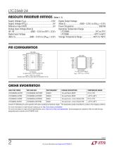
LTC2368-24 ABSOLUTE MAXIMUM RATINGS PIN CONFIGURATION TOP VIEW CHAIN GND OVDD SDO SCK RDL/SDI BUSY GND CNV MS PACKAGE 16-LEAD PLASTIC MSOP TJMAX = 150°C, θJA = 110°C/W DE PACKAGE 16-LEAD (4mm × 3mm) PLASTIC DFN TJMAX = 150°C, θJA = 40°C/W EXPOSED PAD (PIN 17) IS GND, MUST BE SOLDERED TO PCB ORDER INFORMATION LEAD FREE FINISH PART MARKING* PACKAGE DESCRIPTION TEMPERATURE RANGE Consult LTC Marketing for parts specified with wider operating temperature ranges. *The temperature grade is identified by a label on the shipping container. For more information on lead free part marking, go to:...
Abrir o catálogo na página 2
The l denotes the specifications which apply over the full operating temperature range, otherwise specifications are at TA = 25°C. (Note 4) SYMBOL Absolute Input Range (IN+) Absolute Input Range (IN–) Input Differential Voltage Range Analog Input Leakage Current Analog Input Capacitance Input Common Mode Rejection Ratio Sample Mode Hold Mode CONVERTER CHARACTERISTICS The l denotes the specifications which apply over the full operating temperature range, otherwise specifications are at TA = 25°C. (Note 4) SYMBOL LSBRMS LSBRMS LSBRMS LSBRMS Transition Noise Integral Linearity Error...
Abrir o catálogo na página 3
The l denotes the specifications which apply over the full operating temperature range, otherwise specifications are at TA = 25°C and AIN = –1dBFS. (Notes 4, 9) SYMBOL PARAMETER Aperture Delay Aperture Jitter Transient Response Full–Scale Step REFERENCE INPUT The l denotes the specifications which apply over the full operating temperature range, otherwise specifications are at TA = 25°C. (Note 4) SYMBOL Reference Voltage Reference Input Current DIGITAL INPUTS AND DIGITAL OUTPUTS The l denotes the specifications which apply over the full operating temperature range, otherwise specifications...
Abrir o catálogo na página 4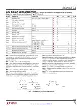
The l denotes the specifications which apply over the full operating temperature range, otherwise specifications are at TA = 25°C. (Note 4) SYMBOL Acquisition Time tACQ = tCYC – tCONV – tBUSYLH (Note 7) Time Between Conversions CNV↑ to BUSY↑ Delay SCK Quiet Time from CNV↑ SDI Setup Time From SCK↑ SDI Hold Time From SCK↑ SCK Period in Chain Mode tSCKCH = tSSDISCK + tDSDO (Note 11) SDO Data Valid Delay from SCK↑ CL = 20pF, OVDD = 5.25V CL = 20pF, OVDD = 2.5V CL = 20pF, OVDD = 1.71V SDO Data Remains Valid Delay from SCK↑ CL = 20pF (Note 7) tDSDOBUSYL SDO Data Valid Delay from BUSY↓ Bus Enable...
Abrir o catálogo na página 5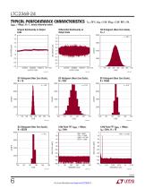
LTC2368-24 TYPICAL PERFORMANCE CHARACTERISTICS fSMPL = 1Msps, N = 1, unless otherwise noted. Integral Nonlinearity vs Output Code Differential Nonlinearity vs Output Code AMPLITUDE (dBFS) AMPLITUDE (dBFS) DC Histogram (Near Zero Scale), N = 65536 DC Histogram (Near Zero Scale), N = 16384 DC Histogram (Near Zero Scale), N = 1024 DC Histogram (Near Zero Scale), N = 16 DC Histogram (Near Zero Scale), N=1
Abrir o catálogo na página 6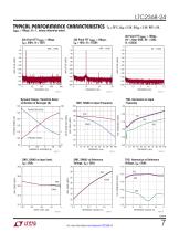
LTC2368-24 TYPICAL PERFORMANCE CHARACTERISTICS fSMPL = 1Msps, N = 1, unless otherwise noted. TA = 25°C, VDD = 2.5V, OVDD = 2.5V, REF = 5V, 8k Point FFT fSMPL = 1Msps, IN+ = Near GND, IN– = GND, N = 65536 AMPLITUDE (dBFS) AMPLITUDE (dBFS) AMPLITUDE (dBFS) DYNAMIC RANGE SNR, SINAD vs Input level, fIN = 2kHz SNR, SINAD vs Reference Voltage, fIN = 2kHz THD, Harmonics vs Input Frequency SNR, SINAD vs Input Frequency Dynamic Range, Transition Noise vs Number of Averages (N) THD, Harmonics vs Reference Voltage, fIN = 2kHz
Abrir o catálogo na página 7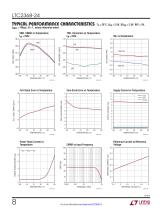
LTC2368-24 TYPICAL PERFORMANCE CHARACTERISTICS fSMPL = 1Msps, N = 1, unless otherwise noted. Full-Scale Error vs Temperature Zero-Scale Error vs Temperature 11 IVDD IREF IOVDD ZERO–SCALE ERROR (LSB) 10 35 TEMPERATURE (°C) Power-Down Current vs Temperature Reference Current vs Reference Voltage CMRR vs Input Frequency Supply Current vs Temperature
Abrir o catálogo na página 8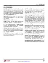
LTC2368-24 PIN FUNCTIONS CHAIN (Pin 1): Chain Mode Selector Pin. When low, the LTC2368-24 operates in normal mode and the RDL/SDI input pin functions to enable or disable SDO. When high, the LTC2368-24 operates in chain mode and the RDL/SDI pin functions as SDI, the daisy-chain serial data input. Logic levels are determined by OVDD. VDD (Pin 2): 2.5V Power Supply. The range of VDD is 2.375V to 2.625V. Bypass VDD to GND with a 10µF ceramic capacitor. GND (Pins 3, 6, 10 and 16): Ground. IN+ (Pin 4): Analog Input. IN+ operates differential with respect to IN– with an IN+ to IN– range of 0V to...
Abrir o catálogo na página 9Todos os catálogos e folhetos técnicos ADI
-
 LTC2068
30 Páginas
-
 LTC6373
34 Páginas
-
 ADL9006
16 Páginas
-
 ADL8104
23 Páginas
-
 AD4115
52 Páginas
-
 ADUM7702
22 Páginas
-
 AD7383
33 Páginas
-
 AD7384
33 Páginas
-
 AD4114
49 Páginas
-
 ADUM7704
22 Páginas
-
 AD7134
86 Páginas
-
 LTspice IV
53 Páginas
-
 New Products Catalog
43 Páginas
-
 RF/IF Amplifiers
9 Páginas
-
 SAR ADC Drivers
2 Páginas
-
 Products for Harsh Environments
4 Páginas
-
 SmartMesh Brochure
8 Páginas
-
 INDUSTRIAL SIGNAL CHAIN
24 Páginas
-
 AUTOMOTIVE ELECTRONIC SOLUTIONS
48 Páginas
-
 µModule® Power Product Family
7 Páginas
-
 Battery Management Solutions
32 Páginas
-
 High Performance DC/DC Controllers
20 Páginas
-
 DC/DC uModule Power Products
32 Páginas
-
 Wireless & RF Solution
36 Páginas
-
 LT2940 - Power and Current Monitor
24 Páginas
-
 LT6656 - 1
18 Páginas
-
 LT3596 - 60V Step-Down LED Driver
22 Páginas


Catálogos arquivados
-
 Automotive & Transportation Solutions
56 Páginas
-
 New Products Catalog
39 Páginas
-
 High Performance DC/DC Controllers
21 Páginas
-
 Power Management for Portable Products
32 Páginas
-
 Power Management for LEDs
24 Páginas
-
 High Speed ADC Products Brochure
14 Páginas