
- Catalogs
- Xiamen Innovacera Advanced Materials Co., Ltd
- 窒化アルミニウム(AIN)ウェハ

- Company
- Products
- Catalogs
- News & Trends
- Exhibitions
窒化アルミニウム(AIN)ウェハ
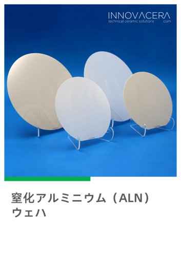
窒化アルミニウム(AIN)ウェハ
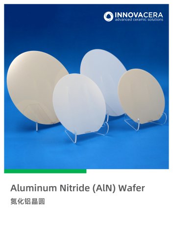
Overview of Aluminum Nitride (AlN) Wafers
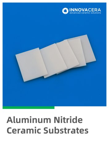
Aluminum Nitride (AlN) is a material known for its high thermal conductivity and excellent thermal stability, making it ideal for high-temperature applications. It is widely used as a substrate material in electronics due to its superior thermal, electrical, and mechanical properties. AlN wafers are particularly suitable for electronic devices such as high-power microwave devices, high-temperature sensors, high-frequency transistors, LEDs, and laser diodes.
Key Properties of AlN
- High thermal conductivity ranging from 170 to 230 W/m·K, up to 9.5 times that of alumina.
- Thermal expansion coefficient similar to silicon, ensuring high reliability and thermal shock resistance for Si chips.
- Excellent electrical insulation with low dielectric constant.
- High mechanical strength (around 450 MPa).
- Superior corrosion resistance against molten metals.
- High purity and non-toxic.
Product Range and Specifications
Innovacera offers a broad range of standard AlN wafers and substrates in sizes including 2", 3", 4", 6", 8", and 12" diameters, with thicknesses from 0.125 mm to 3 mm. The wafer edges are finished by polishing or lapping, and custom sizes are available upon request.
Material Grades and Characteristics
| Property | Unit | AN170 | AN230 |
|---|---|---|---|
| Color | - | Gray | Beige |
| AlN Content | % | >=95 | >=96 |
| Density | g/cm³ | >=3.30 | >=3.28 |
| Bending Strength | MPa | >=400 | >=300 |
| Compressive Strength | MPa | 2500 | 2000 |
| Vickers Hardness (Hv 500g) | GPa | 10.5 | 9 |
| Young's Modulus | GPa | 300 | 300 |
| Thermal Conductivity (@20°C) | W/(m·K) | >=170 | >=220 |
| Specific Heat | KJ/(Kg·K) | 0.74 | 0.73 |
| CTE (Room Temp to 400°C) | 10⁻⁶/K | 4.6 | 4.6 |
| Volume Resistivity (@20°C) | Ω·cm | >=10¹⁴ | >=10¹³ |
| Dielectric Strength | KV/mm | >=16 | >=15 |
| Dielectric Constant (@1MHz) | - | 8.6 | 8.6 |
| Loss Tangent (@1MHz) ×10⁻⁴ | - | 5 | 5 |
Applications
- Semiconductor manufacturing
- Microwave and RF devices
- Optoelectronic devices
- Thermal management solutions
- High-temperature electronic equipment
- LED packaging for circuit cooling and protection
- Power modules such as MOSFET and IGBT
Dimensional and Quality Specifications for 6" and 8" Wafers
- Thermal conductivity: >170, >200, >220 W/(m·K)
- Thermal expansion coefficient: 4–6 ppm/K (300–1200K)
- Sintering aid: Y2O3
- Diameter tolerance: ±0.25 mm
- Notch depth: 1.0 +0.25/-0 mm
- Notch angle: 90° +5/-2°
- Thickness: 400 ± 15 μm
- Thickness tolerance: Premium 0.0127 mm, Standard 0.0254 mm
- Total thickness variation (TTV): Premium 5 μm, Standard 10 μm
- BOW: < ±30 μm
- Warp: < 50 μm
- Surface roughness (Ra): < 50 nm
Surface Finishing Options
- L2S: Double-side polished
- P1S: One side polished + one side lapped
- P2S: Double-side lapped
Available Sizes and Thicknesses
A comprehensive list of square and circular AlN wafers and substrates is provided, ranging from 25.4 mm square to 500 mm diameter, with thicknesses from 0.005 mm up to 25 mm. Each size is available with different surface finishes (L2S, P1S, P2S) to meet various application requirements.
Manufacturer Information
Produced by XIAMEN INNOVACERA ADVANCED MATERIALS CO., LTD, located in Xiamen, China. Contact details include phone: 0086 592 558 9730 and email: [email protected].
Catalog excerpts
n はじめに 窒化アルミニウム(AlN)は高い熱伝導性を持つ材料であり、高温用途に最適です。優れた熱的、 電気的、機械的特性のため、基板材料としてよく使用されます。さらに、AlNウェハは耐熱衝撃性 と熱安定性に優れているため、電子機器や光電子デバイスなどの高温用途に最適です。 AlN ウェハは、高出力マイクロ波デバイ
Open the catalog to page 2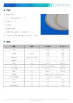
n 応用 • 半導体製造 • マイクロ波およびRFデバイス • 光電子デバイス • 熱管理 • 高温電子機器 • 回路の冷却と保護のためのLEDパッケージ • パワーモジュール (MOSFET, IGBT) 電力モジュール
Open the catalog to page 4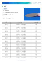
n 規格 表 面 処 理: L2S = 両面研磨 P1S = 片面研磨+片面ラップ仕上げ P2S = 両面ラップ仕上げ 他のサイズも選べます。
Open the catalog to page 5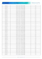
technical ceramic solutions .com
Open the catalog to page 6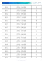
technical ceramic solutions .com
Open the catalog to page 7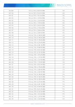
technical ceramic solutions .com
Open the catalog to page 8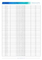
technical ceramic solutions .com
Open the catalog to page 9
XIAMEN INNOVACERA ADVANCED MATERIALS CO.,LTD Block A, 6/F, No.588 Jiahe Road, Torch High-tech Industrial District, Xiamen, China
Open the catalog to page 14All Xiamen Innovacera Advanced Materials Co., Ltd catalogs and technical brochures
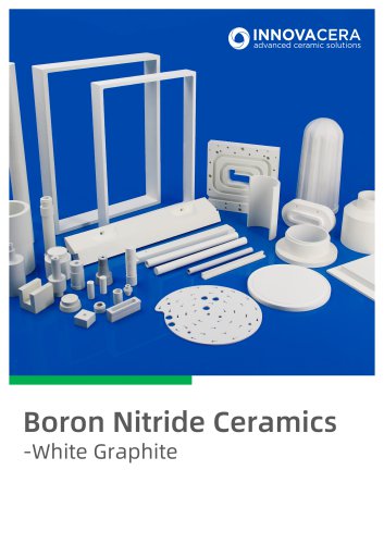 Boron Nitride Ceramic
5 Pages
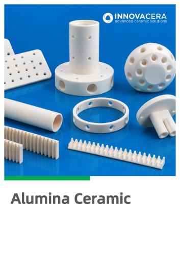 Alumina Ceramic 2026
9 Pages
 アルミセラミック基板
11 Pages
 発熱コア使用上の注意事項
1 Page
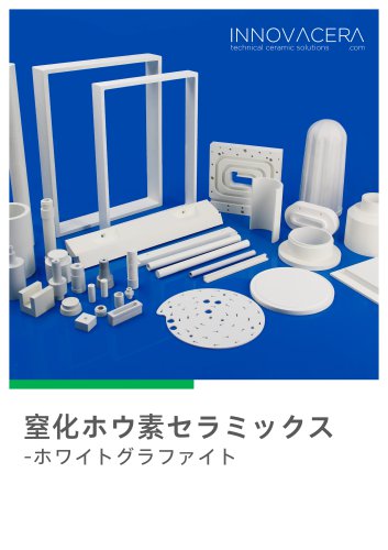 窒化ホウ素セラミックス(BN)
5 Pages
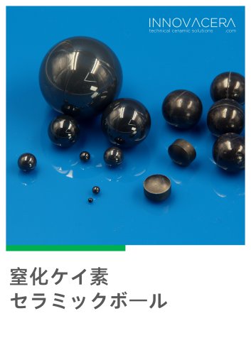 窒化ケイ素セラミックボール
6 Pages
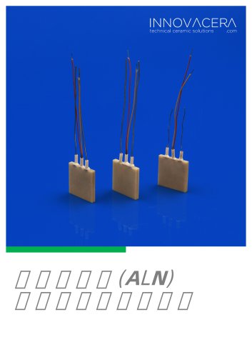 窒化アルミ(ALN)セラミックヒーター
5 Pages
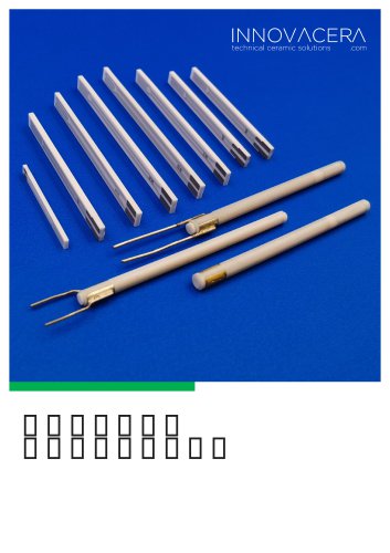 酸素センサー用セラミックヒーター
9 Pages
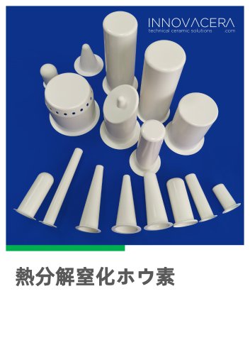 熱分解窒化ホウ素(PBN)
5 Pages
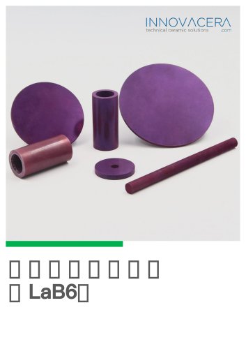 六ホウ化ランタン(LaB6)
5 Pages
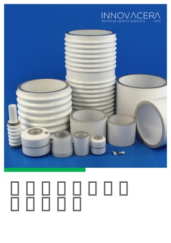 厚膜メタライズドセラミック
4 Pages
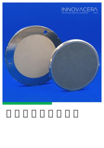 多孔質セラミックス
6 Pages
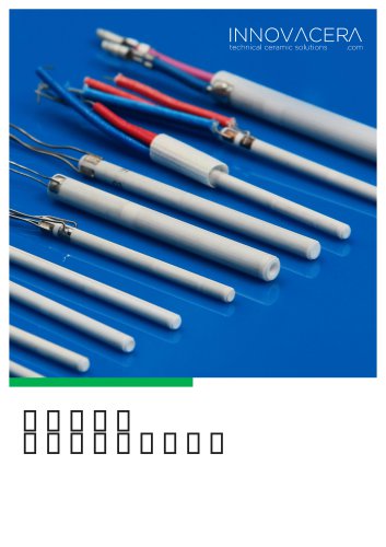 電子工具用セラミックヒーター
7 Pages
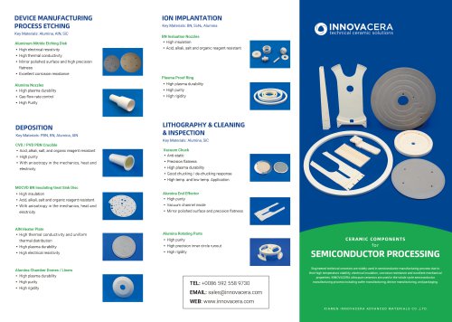
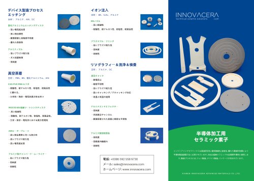 半導体加工用セラミックス
2 Pages
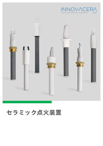 セラミック点火器
8 Pages
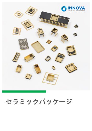 セラミックパッケージ
8 Pages
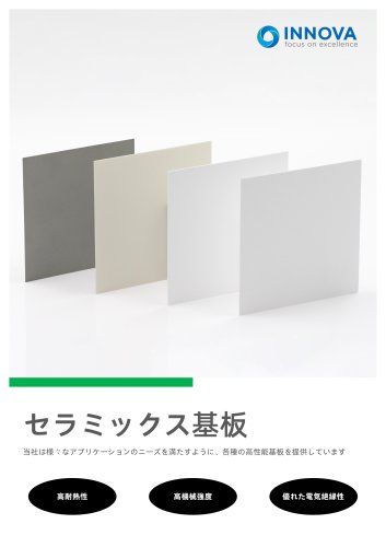 セラミックス基板
9 Pages
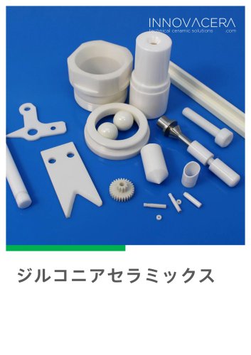 ジルコニアセラミックス(ZrO2)
5 Pages
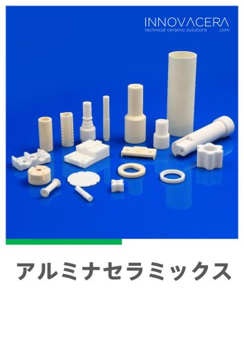 アルミナセラミックス(AI2O3)
9 Pages
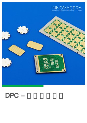 DPC-直接銅めっき
6 Pages
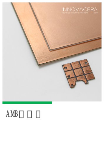 AMB-活性金属ろう付けの紹介
5 Pages
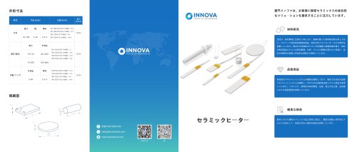 セラミックヒーター
2 Pages
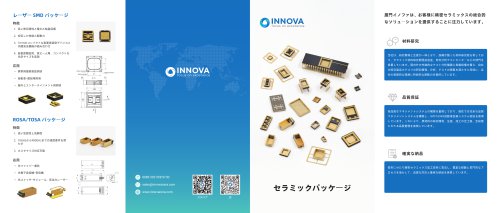 セラミックパッケージ
2 Pages
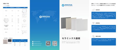 セラミックス基板
2 Pages
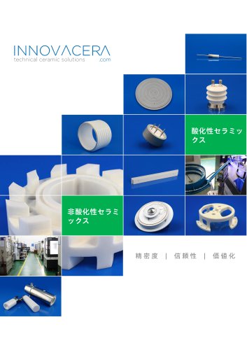 カタログ
カタログ28 Pages
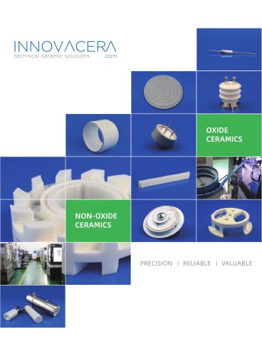 Company Product Catalogue
29 Pages
 ISO 9001:2015
2 Pages
 Beryllia Ceramic
6 Pages
 Ceramic Pellet Igniters
4 Pages
 Biggest Alumina Ceramic Tube
4 Pages
 POROUS CERAMICS|Innovacera
4 Pages




Archived catalogs
 窒化アルミセラミック基板
11 Pages
- Pump
- Industrial pump
- Pump with electric motor
- Stationary pump
- Connector
- Piping
- Self-priming pump
- Chemical pump
- Data connector
- Lubricant pump
- Rectangular housing
- Oil pump
- Electrical power supply connector
- Liquid filter
- Pump for the chemical industry
- Metal connector
- Flap valve
- Check valve
- Positioning table
- Rolling bearing