Si5904DC MOSFETS
1 /9Pages

Si5904DC MOSFETS
1 /9Pages
Catalog excerpts

Dual N-Channel 2.5 V (G-S) MOSFET • Halogen-free According to IEC 61249-2-21 Definition • TrenchFET® Power MOSFET: 2.5 V Rated • Compliant to RoHS Directive 2002/95/EC Lot Traceability and Date Code Part # Code Bottom View N-Channel MOSFET Ordering Information: Si5904DC-T1-E3 (Lead (Pb)-free) Si5904DC-T1-GE3 (Lead (Pb)-free and Halogen-free) N-Channel MOSFET ABSOLUTE MAXIMUM RATINGS TA = 25 °C, unless otherwise noted Parameter Steady State Drain-Source Voltage Gate-Source Voltage Continuous Drain Current (TJ = 150 °C)a Continuous Source Current (Diode Conduction)a Maximum Power Dissipationa Operating Junction and Storage Temperature Range Pulsed Drain Current Soldering Recommendations (Peak THERMAL RESISTANCE RATINGS Parameter Maximum Junction-to-Ambienta Maximum Junction-to-Foot (Drain) Symbol t≤5s Steady State Steady State RthJA RthJF Notes: a. Surface mounted on 1" x 1" FR4 board. b. See reliability manual for profile. The ChipFET is a leadless package. The end of the lead terminal is exposed copper (not plated) as a result of the singulation process in manufacturing. A solder fillet at the exposed copper tip cannot be guaranteed and is not required to ensure adequate bottom side solder interconnection. c. Rework conditions: manual soldering with a soldering iron is not recommended for leadless components. Document Number: 71065 S10-0548-Rev. D, 08-Mar-10
Open the catalog to page 1
Si5904DC Vishay Siliconix SPECIFICATIONS TJ = 25 °C, unless otherwise noted Parameter Test Conditions Static VGS(th) Gate-Body Leakage Zero Gate Voltage Drain Current On-State Drain Currenta Gate Threshold Voltage Drain-Source On-State Resistancea Diode Forward Voltage Forward Transconductancea Dynamicb Total Gate Charge Gate-Source Charge Gate-Drain Charge Turn-On Delay Time Rise Time Turn-Off Delay Time Fall Time Source-Drain Reverse Recovery Time Notes: a. Pulse test; pulse width ≤ 300 µs, duty cycle ≤ 2 %. b. Guaranteed by design, not subject to production testing. Stresses beyond those listed...
Open the catalog to page 2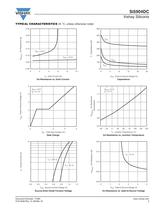
Si5904DC Vishay Siliconix TYPICAL CHARACTERISTICS 25 °C, unless otherwise noted 600 On-Resistance vs. Drain Current Qg - Total Gate Charge (nC) Gate Charge On-Resistance vs. Junction Temperature 0.20 Source-Drain Diode Forward Voltage On-Resistance vs. Gate-to-Source Voltage
Open the catalog to page 3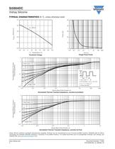
Si5904DC Vishay Siliconix TYPICAL CHARACTERISTICS 25 °C, unless otherwise noted 0.4 Single Pulse Power Normalized Effective Transient Thermal Impedance 2. Per Unit Base = R thJA = 90 °C/W 3. T JM - TA = PDMZthJA(t) Square Wave Pulse Duration (s) Normalized Thermal Transient Impedance, Junction-to-Ambient 2 Normalized Effective Transient Thermal Impedance Square Wave Pulse Duration (s) Normalized Thermal Transient Impedance, Junction-to-Foot Vishay Siliconix maintains worldwide manufacturing capability. Products may be manufactured at one of several qualified locations. Reliability data for Silicon...
Open the catalog to page 4
Package Information Vishay Siliconix 2. Mold gate burrs shall not exceed 0.13 mm per side. 3. Leadframe to molded body offset is horizontal and vertical shall not exceed 4. | Dimensions exclusive of mold gate burrs. 5. No mold flash allowed on the top and bottom lead surface. Document Number: 71151 www.vishay.com
Open the catalog to page 5
Dual-Channel 1206-8 ChipFETr Power MOSFET Recommended Pad Pattern and Thermal Performance INTRODUCTION New Vishay Siliconix ChipFETs in the leadless 1206-8 package feature the same outline as popular 1206-8 resistors and capacitors but provide all the performance of true power semiconductor devices. The 1206-8 ChipFET has the same footprint as the body of the LITTLE FOOTR TSOP-6, and can be thought of as a leadless TSOP-6 for purposes of visualizing board area, but its thermal performance bears comparison with the much larger SO-8. This technical note discusses the dual ChipFET 1206-8 pin-out,...
Open the catalog to page 6
AN812 Vishay Siliconix Front of Board Junction-to-Foot Thermal Resistance (the Package Performance) Thermal performance for the 1206-8 ChipFET measured as junction-to-foot thermal resistance is 30_C/W typical, 40_C/W maximum for the dual device. The “foot” is the drain lead of the device as it connects with the body. This is identical to the dual SO-8 package RQjf performance, a feat made possible by shortening the leads to the point where they become only a small part of the total footprint area. Junction-to-Ambient Thermal Resistance (dependent on pcb size) The typical RQja for the dual-channel...
Open the catalog to page 7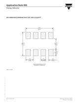
Vishay Siliconix RECOMMENDED MINIMUM PADS FOR 1206-8 ChipFET® Recommended Minimum Pads www.vishay.com Document Number: 72593
Open the catalog to page 8
Legal Disclaimer Notice www.vishay.com Disclaimer ALL PRODUCT, PRODUCT SPECIFICATIONS AND DATA ARE SUBJECT TO CHANGE WITHOUT NOTICE TO IMPROVE RELIABILITY, FUNCTION OR DESIGN OR OTHERWISE. Vishay Intertechnology, Inc., its affiliates, agents, and employees, and all persons acting on its or their behalf (collectively, “Vishay”), disclaim any and all liability for any errors, inaccuracies or incompleteness contained in any datasheet or in any other disclosure relating to any product. Vishay makes no warranty, representation or guarantee regarding the suitability of the products for any particular...
Open the catalog to page 9All VISHAY catalogs and technical brochures
 VS-E5TH1506THN3
8 Pages
 VS-E5TX1506THN3
8 Pages
 VS-E5TH3006THN3
8 Pages
 VS-E5TX3006THN3
8 Pages
 VS-E5PH3006LHN3
6 Pages
 VS-E5PX3006LHN3
6 Pages
 VS-E5PH6006LHN3
6 Pages
 VS-E5PX6006LHN3
6 Pages
 VS-E5PH7506LHN3
6 Pages
 VS-E5PX7506LHN3
6 Pages
 VCNL36825T
16 Pages
 VS-E5TH1506-M3
7 Pages
 VS-E5TX1506-M3
7 Pages
 VS-E5TH3006-M3
7 Pages
 VS-E5TX3006-M3
7 Pages
 VS-E5PH3006L-N3
8 Pages
 VS-E5PX3006L-N3
7 Pages
 VS-E5PH6006L-N3
7 Pages
 VS-E5PX6006L-N3
7 Pages
 VS-E5PH7506L-N3
7 Pages
 VS-E5PX7506L-N3
7 Pages
 VS-C04ET07T-M3
5 Pages
 VS-C06ET07T-M3
5 Pages
 VS-C08ET07T-M3
5 Pages
 VS-C10ET07T-M3
5 Pages
 VS-C12ET07T-M3
5 Pages
 VS-C16CP07L-M3
5 Pages
 VS-C16ET07T-M3
5 Pages
 VS-C20CP07L-M3
5 Pages
 VS-C20ET07T-M3
5 Pages
 VS-C40CP07L-M3
5 Pages
 P11H
P11H7 Pages
 IHTH-1500MZ-5A
4 Pages
 IHTH-1500TZ-5A
4 Pages
 MFU AT SERIES
8 Pages
 T24
T247 Pages
 CRHA
CRHA4 Pages
 IHXL-1500VZ-5A
5 Pages
 Power Modules
32 Pages
 Bare Die
29 Pages
 TMBS® Rectifiers
2 Pages
 XOSM-531 OSCILLATORS
3 Pages
 IHLP2525EZ-01 INDUCTORS
4 Pages
 HYBRIDS & SUBSTRATES HP - MT
2 Pages
 Fuses HCTF CP Series
5 Pages
 XT49S CRYSTALS
3 Pages
 VOM1271 SOLID-STATE RELAYS
7 Pages
 Chip Antenna
6 Pages
 2381 691 90001/HUMIDITY-SENS-E
2 Pages
 Inductors - Power Inductors
2 Pages
 Capacitors - Ceramic
7 Pages
 Capacitors - Radial
5 Pages


Archived catalogs
 RC Thermal Model for 2N7002K
3 Pages
 MLCC Product Road Map
4 Pages


- Connector
- Display module
- Proximity switch
- Rectangular connector
- Switching relay
- LED display panel
- Position transducer
- Inductive proximity sensor
- Transceiver module
- Electronic display panel
- Linear position transmitter
- Radio antenna
- Analog position transducer
- SMT connector
- No-contact position sensor
- Medical equipment display
- Potentiometer
- Ceramic capacitor