
Catalog excerpts
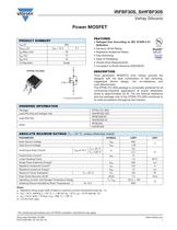
Document Number: 91389 www.vishay.com S10-2433-Rev. B, 25-Oct-10 1 Power MOSFET IRFBF30S, SiHFBF30S Vishay Siliconix FEATURES • Halogen-free According to IEC 61249-2-21 Definition • Dynamic dV/dt Rating • Repetitive Avalanche Rated • Fast Switching • Ease of Paralleling • Simple Drive Requirements • Compliant to RoHS Directive 2002/95/EC DESCRIPTION Third generation MOSFETs from Vishay provide the designer with the best combination of fast switching, ruggedized device design, low on-resistance and cost-effectiveness. The D2PAK (TO-263) package is universially preferred for all commercial-industrial applications at power dissipation levels to approximately 50 W. The low thermal resistance and low package cost of the D2PAK (TO-263) contribute to its wide acceptance throughout the industry. Notes a. Repetitive rating; pulse width limited by maximum junction temperature (see fig. 11). b. VDD = 50 V, starting TJ = 25 °C, L = 36 mH, Rg = 25 ƒÇ, IAS = 3.6 A (see fig. 12). c. ISD „T 3.6 A, dI/dt „T 70 A/ìs, VDD „T 600, TJ „T 150 °C. d. 1.6 mm from case. PRODUCT SUMMARY VDS (V) 900 RDS(on) (ƒÇ) VGS = 10 V 3.7 Qg (Max.) (nC) 78 Qgs (nC) 10 Qgd (nC) 42 Configuration Single N-Channel MOSFET G D S D2PAK (TO-263) G D S ORDERING INFORMATION Package D2PAK (TO-263) Lead (Pb)-free and Halogen-free SiHFBF30S-GE3 Lead (Pb)-free IRFBF30SPbF SiHFBF30S-E3 SnPb IRFBF30S SiHFBF30S ABSOLUTE MAXIMUM RATINGS (TC = 25 °C, unless otherwise noted) PARAMETER SYMBOL LIMIT UNIT Drain-Source Voltage VDS 900 V Gate-Source Voltage VGS ± 20 Continuous Drain Current VGS at 10 V TC = 25 °C ID 3.6 TC = 100 °C 2.3 A Pulsed Drain Currenta IDM 14 Linear Derating Factor 1.0 W/°C Single Pulse Avalanche Energyb EAS 250 mJ Repetitive Avalanche Currenta IAR 3.6 A Repetitive Avalanche Energya EAR 13 mJ Maximum Power Dissipation TC = 25 °C PD 125 W Peak Diode Recovery dV/dtc dV/dt 1.5 V/ns Operating Junction and Storage Temperature Range TJ, Tstg - 55 to + 150 °C Soldering Recommendations (Peak Temperature) for 10 s 300d * Pb containing terminations are not RoHS compliant, exemptions may apply
Open the catalog to page 1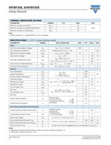
www.vishay.com Document Number: 91389 2 S10-2433-Rev. B, 25-Oct-10 IRFBF30S, SiHFBF30S Vishay Siliconix Note a. When mounted on 1" square PCB (FR-4 or G-10 material). Notes a. Repetitive rating; pulse width limited by maximum junction temperature (see fig. 11). b. Pulse width „T 300 ìs; duty cycle „T 2 %. THERMAL RESISTANCE RATINGS PARAMETER SYMBOL TYP. MAX. UNIT Maximum Junction-to-Ambient RthJA - 62 Maximum Junction-to-Ambient (PCB Mount)a RthJA - 40 °C/W Maximum Junction-to-Case (Drain) RthJC - 1.0 SPECIFICATIONS (TJ = 25 °C, unless otherwise noted) PARAMETER SYMBOL TEST CONDITIONS MIN....
Open the catalog to page 2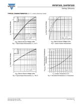
Document Number: 91389 www.vishay.com S10-2433-Rev. B, 25-Oct-10 3 IRFBF30S, SiHFBF30S Vishay Siliconix TYPICAL CHARACTERISTICS (25 °C, unless otherwise noted) Fig. 1 - Typical Output Characteristics, TC = 25 °C Fig. 2 -Typical Output Characteristics, TC = 150 °C Fig. 3 - Typical Transfer Characteristics Fig. 4 - Normalized On-Resistance vs. Temperature
Open the catalog to page 3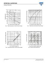
www.vishay.com Document Number: 91389 4 S10-2433-Rev. B, 25-Oct-10 IRFBF30S, SiHFBF30S Vishay Siliconix Fig. 5 - Typical Capacitance vs. Drain-to-Source Voltage Fig. 6 - Typical Gate Charge vs. Gate-to-Source Voltage Fig. 7 - Typical Source-Drain Diode Forward Voltage Fig. 8 - Maximum Safe Operating Area
Open the catalog to page 4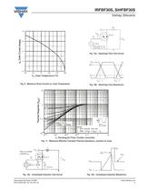
Document Number: 91389 www.vishay.com S10-2433-Rev. B, 25-Oct-10 5 IRFBF30S, SiHFBF30S Vishay Siliconix Fig. 9 - Maximum Drain Current vs. Case Temperature Fig. 10a - Switching Time Test Circuit Fig. 10b - Switching Time Waveforms Fig. 11 - Maximum Effective Transient Thermal Impedance, Junction-to-Case Fig. 12a - Unclamped Inductive Test Circuit Fig. 12b - Unclamped Inductive Waveforms Pulse width 1 ìs Duty factor 0.1 % RD VGS Rg D.U.T. 10 V +- VDS VDD VDS 90 % 10 % VGS td(on) tr td(off) tf Rg IAS tp 0.01 Ù D.U.T L VDS + - VDD A 10 V Vary tp to obtain required IAS IAS VDS VDD VDS tp
Open the catalog to page 5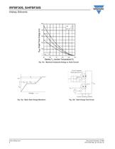
www.vishay.com Document Number: 91389 6 S10-2433-Rev. B, 25-Oct-10 IRFBF30S, SiHFBF30S Vishay Siliconix Fig. 12c - Maximum Avalanche Energy vs. Drain Current Fig. 13a - Basic Gate Charge Waveform Fig. 13b - Gate Charge Test Circuit QGS QGD QG VG Charge 10 V D.U.T. 3 mA VGS VDS IG ID 0.3 ìF 0.2 ìF 50 kÙ 12 V Current regulator Current sampling resistors Same type as D.U.T. + -
Open the catalog to page 6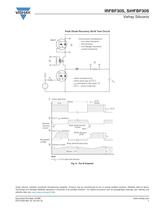
Document Number: 91389 www.vishay.com S10-2433-Rev. B, 25-Oct-10 7 IRFBF30S, SiHFBF30S Vishay Siliconix Fig. 9 - For N-Channel Vishay Siliconix maintains worldwide manufacturing capability. Products may be manufactured at one of several qualified locations. Reliability data for Silicon Technology and Package Reliability represent a composite of all qualified locations. For related documents such as package/tape drawings, part marking, and reliability data, see www.vishay.com/ppg?91389. P.W. Period dI/dt Diode recovery dV/dt Ripple 5 % Body diode forward drop Re-applied voltage Reverse...
Open the catalog to page 7
Document Number: 91000 www.vishay.com Revision: 11-Mar-11 1 Disclaimer Legal Disclaimer Notice Vishay ALL PRODUCT, PRODUCT SPECIFICATIONS AND DATA ARE SUBJECT TO CHANGE WITHOUT NOTICE TO IMPROVE RELIABILITY, FUNCTION OR DESIGN OR OTHERWISE. Vishay Intertechnology, Inc., its affiliates, agents, and employees, and all persons acting on its or their behalf (collectively, “Vishay”), disclaim any and all liability for any errors, inaccuracies or incompleteness contained in any datasheet or in any other disclosure relating to any product. Vishay makes no warranty, representation or guarantee...
Open the catalog to page 8All VISHAY catalogs and technical brochures
-
VS-E5TH1506THN3
8 Pages
-
VS-E5TX1506THN3
8 Pages
-
VS-E5TH3006THN3
8 Pages
-
VS-E5TX3006THN3
8 Pages
-
VS-E5PH3006LHN3
6 Pages
-
VS-E5PX3006LHN3
6 Pages
-
VS-E5PH6006LHN3
6 Pages
-
VS-E5PX6006LHN3
6 Pages
-
VS-E5PH7506LHN3
6 Pages
-
VS-E5PX7506LHN3
6 Pages
-
VCNL36825T
16 Pages
-
VS-E5TH1506-M3
7 Pages
-
VS-E5TX1506-M3
7 Pages
-
VS-E5TH3006-M3
7 Pages
-
VS-E5TX3006-M3
7 Pages
-
VS-E5PH3006L-N3
8 Pages
-
VS-E5PX3006L-N3
7 Pages
-
VS-E5PH6006L-N3
7 Pages
-
VS-E5PX6006L-N3
7 Pages
-
VS-E5PH7506L-N3
7 Pages
-
VS-E5PX7506L-N3
7 Pages
-
VS-C04ET07T-M3
5 Pages
-
VS-C06ET07T-M3
5 Pages
-
VS-C08ET07T-M3
5 Pages
-
VS-C10ET07T-M3
5 Pages
-
VS-C12ET07T-M3
5 Pages
-
VS-C16CP07L-M3
5 Pages
-
VS-C16ET07T-M3
5 Pages
-
VS-C20CP07L-M3
5 Pages
-
VS-C20ET07T-M3
5 Pages
-
VS-C40CP07L-M3
5 Pages
-
P11H
7 Pages
-
IHTH-1500MZ-5A
4 Pages
-
IHTH-1500TZ-5A
4 Pages
-
MFU AT SERIES
8 Pages
-
T24
7 Pages
-
CRHA
4 Pages
-
IHXL-1500VZ-5A
5 Pages
-
Power Modules
32 Pages
-
Bare Die
29 Pages
-
TMBS® Rectifiers
2 Pages
-
XOSM-531 OSCILLATORS
3 Pages
-
IHLP2525EZ-01 INDUCTORS
4 Pages
-
HYBRIDS & SUBSTRATES HP - MT
2 Pages
-
Fuses HCTF CP Series
5 Pages
-
XT49S CRYSTALS
3 Pages
-
VOM1271 SOLID-STATE RELAYS
7 Pages
-
Si5904DC MOSFETS
9 Pages
-
Chip Antenna
6 Pages
-
2381 691 90001/HUMIDITY-SENS-E
2 Pages
-
Inductors - Power Inductors
2 Pages
-
Capacitors - Ceramic
7 Pages
-
Capacitors - Radial
5 Pages
Archived catalogs
-
RC Thermal Model for 2N7002K
3 Pages
-
MLCC Product Road Map
4 Pages


