DG406, DG407 ANALOG SWITCHES AND MULTIPLEXERS
1 /16Pages

DG406, DG407 ANALOG SWITCHES AND MULTIPLEXERS
1 /16Pages
Catalog excerpts
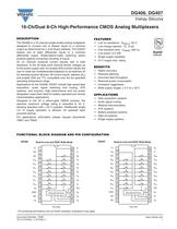
16-Ch/Dual 8-Ch High-Performance CMOS Analog Multiplexers DESCRIPTION The DG406 is a 16 channel single-ended analog multiplexer designed to connect one of sixteen inputs to a common output as determined by a 4-bit binary address. The DG407 selects one of eight differential inputs to a common differential output. Break-before-make switching action protects against momentary shorting of inputs. An on channel conducts current equally well in both directions. In the off state each channel blocks voltages up to the power supply rails. An enable (EN) function allows the user to reset the multiplexer/demultiplexer to all switches off for stacking several devices. All control inputs, address (Ax) and enable (EN) are TTL compatible over the full specified operating temperature range. Applications for the DG406, DG407 include high speed data acquisition, audio signal switching and routing, ATE systems, and avionics. High performance and low power dissipation make them ideal for battery operated and remote instrumentation applications. Designed in the 44 V silicon-gate CMOS process, the absolute maximum voltage rating is extended to 44 V, allowing operation with ± 20 V supplies. Additionally single (12 V) supply operation is allowed. An epitaxial layer prevents latchup. For applications information please request documents 70601 and 70604. Low on-resistance - RDS(on): 50 Low charge injection - Q: 15 pC Fast transition time - tTRANS: 200 ns Low power: 0.2 mW Single supply capability • 44 V supply max. rating Pb-free Available RoHS* COMPLIANT Higher accuracy Reduced glitching Improved data throughput Reduced power consumption Increased ruggedness Wide supply ranges: ± 5 V to ± 20 V Data acquisition systems Audio signal routing Medical instrumentation ATE systems Battery powered systems High-rel systems Single supply systems FUNCTIONAL BLOCK DIAGRAM AND PIN CONFIGURATION DG406 Dual-In-Line and SOIC Wide-Body V+ Dual-In-Line and SOIC Wide-Body * Pb containing terminations are not RoHS compliant, exemptions may apply Document Number: 70061 S11-0179-Rev. J, 07-Feb-11
Open the catalog to page 1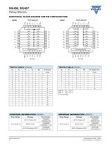
DG406, DG407 Vishay Siliconix FUNCTIONAL BLOCK DIAGRAM AND PIN CONFIGURATION PLCC and LCC ORDERING INFORMATION (DG406) Temp. Range Part Number Logic “0” = VAL 0.8 V Logic “1” = VAH 2.4 V X = Do not Care Temp. Range Part Number
Open the catalog to page 2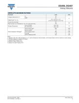
DG406, DG407 Vishay Siliconix ABSOLUTE MAXIMUM RATINGS Parameter Voltages Referenced to VDigital Inputs Current (Any terminal) Peak Current, S or D (Pulsed at 1 ms, 10 % duty cycle max.) Storage Temperature Limit 44 25 (V-) - 2 to (V+) + 2 V or 20 mA, whichever occurs first 30 100 Power Dissipation (Package)b Notes: a. Signals on SX, DX or INX exceeding V+ or V- will be clamped by internal diodes. Limit forward diode current to maximum current ratings. b. All leads soldered or welded to PC board. c. Derate 6 mW/°C above 75°C. d. Derate 12 mW/°C above 75°C. e. Derate 13.5 mW/°C above 75°C .
Open the catalog to page 3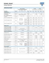
DG406, DG407 Vishay Siliconix SPECIFICATIONSa Test Conditions Unless Otherwise Specified V+ = 15 V, V- = - 15 V VAL = 0.8 V, VAH = 2.4 Vf VD = ± 10 V, IS = - 10 mA sequence each switch on Full Room Full Parameter Analog Switch Analog Signal Rangee Drain-Source On-Resistance RDS(on) Matching Between Channelsg Source Off Leakage Current Drain Off Leakage Current Drain On Leakage Current VS = VD = ± 10 sequence each switch on Room Full Room Full Room Full Room Full Room Full Digital Control Logic High Input Voltage Logic Low Input Voltage Logic High Input Current Logic Low Input Current Logic Input...
Open the catalog to page 4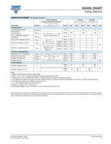
DG406, DG407 Vishay Siliconix SPECIFICATIONSa (for Single Supply) Parameter Analog Switch Analog Signal Rangee Drain-Source On-Resistance RDS(on) Matching Between Channelsg Source Off Leakage Current Test Conditions Unless Otherwise Specified V+ = 12 V, V- = 0 V VAL = 0.8 V, VAH = 2.4 Vf Drain Off Leakage Current Drain On Leakage Current RDS(on) RDS(on) IS(off) ID(off) ID(on) A Suffix D Suffix - 55 °C to 125 °C - 40 °C to 85 °C Temp.b VD = 3 V, 10 V, IS = - 1 mA sequence each switch on VEN = 0 V VD = 10 V or 0.5 V VS = 0.5 V or 10 V VS = VD = ± 10 sequence each switch on Dynamic Characteristics...
Open the catalog to page 5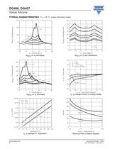
DG406, DG407 Vishay Siliconix TYPICAL CHARACTERISTICS (TA = 25 °C, unless otherwise noted) 160 V+ = 15 V V- = - 15 V VS = - VD for ID(off) VD = V S(open) for ID(on) ID(on), ID(off) ID , IS Leakage Currents vs. Analog Voltage VS , V D - Source Drain Voltage (V) VSUPPLY - Supply Voltage (V) Switching Times vs. Bipolar Supplies
Open the catalog to page 6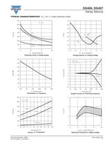
DG406, DG407 Vishay Siliconix TYPICAL CHARACTERISTICS (TA = 25 °C, unless otherwise noted) 70 Switching Times vs. Single Supply Charge Injection vs. Analog Voltage Supply Currents vs. Switching Frequency VSUPPLY - Supply Voltage (V) Switching Threshold vs. Supply Voltage
Open the catalog to page 7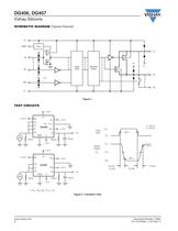
DG406, DG407 Vishay Siliconix SCHEMATIC DIAGRAM (Typical Channel) Decode/ Drive Logic Input Figure 2. Transition Time
Open the catalog to page 8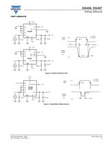
DG406, DG407 Vishay Siliconix TEST CIRCUITS + 15 V V+ A3 Logic Input Switch Output Figure 3. Enable Switching Time + 15 V Logic Input Switch Output Figure 4. Break-Before-Make Interval
Open the catalog to page 9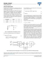
DG406, DG407 Vishay Siliconix APPLICATIONS HINTS Sampling speed is limited by two consecutive events: the transition time of the multiplexer, and the settling time of the sampled signal at the output. For the DG406 then, at room temp and for 12-bit accuracy, using the maximum limits: tTRANS is given on the data sheet. Settling time at the load depends on several parameters: RDS(on) of the multiplexer, source impedance, multiplexer and load capacitances, charge injection of the multiplexer and accuracy desired. The settling time for the multiplexer alone can be derived from the model shown in...
Open the catalog to page 10
Package Information Vishay Siliconix
Open the catalog to page 11
Package Information Vishay Siliconix PLCC: 28-LEAD D-SQUARE
Open the catalog to page 12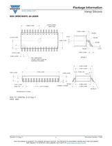
Package Information Vishay Siliconix SURFACE POLISHED THIS DOCUMENT IS SUBJECT TO CHANGE WITHOUT NOTICE. THE PRODUCTS DESCRIBED HEREIN AND THIS DOCUMENT ARE SUBJECT TO SPECIFIC DISCLAIMERS, SET FORTH AT www.vishay.com/doc791000
Open the catalog to page 13All VISHAY catalogs and technical brochures
 VS-E5TH1506THN3
8 Pages
 VS-E5TX1506THN3
8 Pages
 VS-E5TH3006THN3
8 Pages
 VS-E5TX3006THN3
8 Pages
 VS-E5PH3006LHN3
6 Pages
 VS-E5PX3006LHN3
6 Pages
 VS-E5PH6006LHN3
6 Pages
 VS-E5PX6006LHN3
6 Pages
 VS-E5PH7506LHN3
6 Pages
 VS-E5PX7506LHN3
6 Pages
 VCNL36825T
16 Pages
 VS-E5TH1506-M3
7 Pages
 VS-E5TX1506-M3
7 Pages
 VS-E5TH3006-M3
7 Pages
 VS-E5TX3006-M3
7 Pages
 VS-E5PH3006L-N3
8 Pages
 VS-E5PX3006L-N3
7 Pages
 VS-E5PH6006L-N3
7 Pages
 VS-E5PX6006L-N3
7 Pages
 VS-E5PH7506L-N3
7 Pages
 VS-E5PX7506L-N3
7 Pages
 VS-C04ET07T-M3
5 Pages
 VS-C06ET07T-M3
5 Pages
 VS-C08ET07T-M3
5 Pages
 VS-C10ET07T-M3
5 Pages
 VS-C12ET07T-M3
5 Pages
 VS-C16CP07L-M3
5 Pages
 VS-C16ET07T-M3
5 Pages
 VS-C20CP07L-M3
5 Pages
 VS-C20ET07T-M3
5 Pages
 VS-C40CP07L-M3
5 Pages
 P11H
P11H7 Pages
 IHTH-1500MZ-5A
4 Pages
 IHTH-1500TZ-5A
4 Pages
 MFU AT SERIES
8 Pages
 T24
T247 Pages
 CRHA
CRHA4 Pages
 IHXL-1500VZ-5A
5 Pages
 Power Modules
32 Pages
 Bare Die
29 Pages
 TMBS® Rectifiers
2 Pages
 XOSM-531 OSCILLATORS
3 Pages
 IHLP2525EZ-01 INDUCTORS
4 Pages
 HYBRIDS & SUBSTRATES HP - MT
2 Pages
 Fuses HCTF CP Series
5 Pages
 XT49S CRYSTALS
3 Pages
 VOM1271 SOLID-STATE RELAYS
7 Pages
 Si5904DC MOSFETS
9 Pages
 Chip Antenna
6 Pages
 2381 691 90001/HUMIDITY-SENS-E
2 Pages
 Inductors - Power Inductors
2 Pages
 Capacitors - Ceramic
7 Pages
 Capacitors - Radial
5 Pages


Archived catalogs
 RC Thermal Model for 2N7002K
3 Pages
 MLCC Product Road Map
4 Pages


- Connector
- Display module
- Proximity switch
- Rectangular connector
- Switching relay
- Capacitor
- LED display panel
- Position transducer
- Inductive proximity sensor
- Transceiver module
- Electronic display panel
- Linear position transmitter
- Radio antenna
- Analog position transducer
- SMT connector
- No-contact position sensor
- Medical equipment display
- Potentiometer
- Ceramic capacitor