- Catalogs
- Vectron International
- VCC1 Crystal Oscillator (XO)
VCC1 Crystal Oscillator (XO)
1 /10Pages

VCC1 Crystal Oscillator (XO)
1 /10Pages
Catalog excerpts
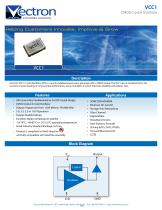
VCC1 CMOS Crystal Oscillator VCC1 Description Vectron’s VCC1 Crystal Oscillator (XO) is a quartz stabilized square wave generator with a CMOS output. The VCC1 uses a fundamental or 3rd overtone crystal resulting in very low jitter performance, and a monolithic IC which improves reliability and reduces cost. Ultra Low Jitter, Fundamental or 3rd OT Crystal Design CMOS Output Crystal Oscillator Output Frequencies from 1.024 MHz to 190.000 MHz 5.0, 3.3, 2.5 or 1.8 V Operation Output Disable Feature Excellent 20ppm temperature stability -10/70°C , -40/85°C or -55/125°C operating temperature Small Industry Standard Package, 5x7mm Product is compliant to RoHS directive and fully compatible with lead free assembly SONET/SDH/DWDM Ethernet, GE, SynchE Storage Area Networking Fiber Channel Digital Video Broadband Access Base Stations, Picocells Driving A/D’s, D/A’s, FPGA’s Test and Measurement COTS Block Diagram Output Vectron International • 267 Lowell Road, Hudson, NH 03051 • Tel: 1-88-VECTRON-1 • http://www.vectron.com Page1
Open the catalog to page 1
Performance Specifications Table 1. Electrical Performance, 5V Option Parameter Current, Output Disabled Stability , (Ordering Option) Output Logic Levels Output Logic High Output Logic Low Output Logic High Drive Output Logic Low Drive Output Rise /Fall Time <20.000MHz 20.000 to 50.000MHz 50.001 to 125.000MHz Output Leakage, Output Disabled Period Jitter RMS Peak-Peak Enable/Disable Output Enable/Disable7 Output Enable Output Disable Disable time Enable Internal Pull-Up Resistor Start-Up Time Operating Temp, (Ordering Option) The power supply should have by-pass capacitors as close to the supply...
Open the catalog to page 2
Performance Specifications Table 2. Electrical Performance, 3.3V Option Parameter Maximum Voltage Current, Output Disabled Nominal Frequency Output Logic Levels Output Logic High Output Logic Low Output Logic High Drive Output Logic Low Drive Output Rise /Fall Time <20.000MHz 20.000 to 50.000MHz 50.001 to 90.000MHz 90.001 to 190.000MHz Output Leakage, Output Disabled2,5 Duty Cycle Period Jitter RMS Peak-Peak Enable/Disable Output Enable/Disable7 Output Enable Output Disable Disable time Enable Internal Pull-Up Resistor Start-Up Time Operating Temp, (Ordering Option) The power supply should have...
Open the catalog to page 3
Performance Specifications Table 3. Electrical Performance, 2.5V Option Parameter Maximum Voltage Current, Output Disabled Nominal Frequency Output Logic Levels Output Logic High Output Logic Low Output Logic High Drive Output Logic Low Drive Output Logic High Drive5 Output Logic Low Drive5 Output Leakage, Output Disabled Period Jitter RMS Peak-Peak Output Enable/Disable Output Enable Output Disable Disable time Enable Internal Pull-Up Resistor Start-Up Time Operating Temp, (Ordering Option) The power supply should have by-pass capacitors as close to the supply and to ground as possible, for...
Open the catalog to page 4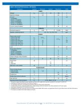
Performance Specifications Table 4. Electrical Performance, 1.8V Option Parameter Maximum Voltage Current, Output Disabled Nominal Frequency Stability , (Ordering Option) Outputs Output Logic Levels2,3 Output Logic High Output Logic Low Output Logic High Drive Output Logic Low Drive Output Logic High Drive5 Output Logic Low Drive5 Output Rise /Fall Time <20.000MHz 20.000 to 50.000MHz 50.001 to 90.000MHz 90.000 to 172.000MHz Output Leakage, Output Disabled Duty Cycle Period Jitter RMS Peak-{eak Enable/Disable Output Enable/Disable8 Output Enable Output Disable Disable time Enable Internal Pull-Up...
Open the catalog to page 5
Test Diagram and Waveform tR IDD + VDD + Period Fig 1: Test Circuit Outline Drawing & Pad Layout Recommended Soldering Pad Layout Dimensions in mm VCC1-XXX Part Number XXMXXX Frequency Date Code YYWW C Enable Disable Case and Electrical Ground Alternate Package Design Power Supply Voltage Vectron International • 267 Lowell Road, Hudson, NH 03051 • Tel: 1-88-VECTRON-1 • http://www.vectron.com Page6
Open the catalog to page 6
Reliability VI qualification includes aging at various extreme temperatures, shock and vibration, temperature cycling, and IR reflow simulation. The VCC1 family is capable of meeting the following qualification tests: Table 6. Environmental Compliance Parameter Mechanical Shock Mechanical Vibration Temperature Cycle Gross and Fine Leak Moisture Sensitivity Level Contact Pads Gold over Nickel Although ESD protection circuitry has been designed into the VCC1 proper precautions should be taken when handling and mounting. VI employs a human body model (HBM) and a charged device model (CDM) for ESD...
Open the catalog to page 7
The VCC1 is qualified to meet the JEDEC standard for Pb-Free assembly. The temperatures and time intervals listed are based on the Pb-Free small body requirements. The VCC1 device is hermetically sealed so an aqueous wash is not an issue. Table 9. Reflow Profile Parameter PreHeat Time Ts-min Ts-max Time To Peak Temperature Ramp Down Tape and Reel Tape & Reel (EIA-481-2-A) Table 10. Tape and Reel Information Tape Dimensions (mm) Vectron International • 267 Lowell Road, Hudson, NH 03051 • Tel: 1-88-VECTRON-1 • http://www.vectron.com Page8
Open the catalog to page 8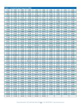
Table 11. Standard Output Frequencies (MHz) 1.544 Vectron International • 267 Lowell Road, Hudson, NH 03051 • Tel: 1-88-VECTRON-1 • http://www.vectron.com Page9
Open the catalog to page 9
Ordering Information VCC1- B3B- xxMxxxxxxx Product 5x7 Crystal Oscillator Stability A: ±100ppm over -10/70°C B: ±50ppm over -10/70°C C: ±100ppm over -40/85°C D: ±50ppm over -40/85°C E: ±25ppm over -10/70°C F: ±25ppm over -40/85°C K: ±32ppm over -10/70°C O: ±32ppm over -40/85°C P: ±100ppm over -55/125°C R: ±50ppm over -55/125°C Electrical Options: 3: Tri-state 45/55% Duty Cycle The following codes are not recommended for new designs 0: No Tri-state, 40/60% Duty 1: Tri-state, 40/60% Duty 2: No tri-state, 45/55% Duty 5: Enable, 40/60% Duty 6: Enable, 45/55% Duty Example: VCC1-B3B-125M000000 *Note:...
Open the catalog to page 10All Vectron International catalogs and technical brochures
 PX-340
4 Pages
 PX-422
6 Pages
 M55310/16
4 Pages
 M55310/21
5 Pages
 M55310/30
6 Pages
 CD-700 A Quartz Stabilized PLL
20 Pages
 Timing Module Brochure
5 Pages
 OX-171 Holdover Oscillators
6 Pages
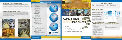 SAW Filter Products
2 Pages
 Military Products
9 Pages
 VXA7 Standard Crystal
2 Pages


Archived catalogs
 FX-702 Frequency Translation
7 Pages
 2009 catalog
8 Pages
 SAW Product Brochure
8 Pages


