
- Catalogs
- Trenz Electronic GmbH
- Configuring Xilinx FPGAs with SPI Serial Flash

Configuring Xilinx FPGAs with SPI Serial Flash

Configuring Xilinx FPGAs with SPI Serial Flash
This document provides a comprehensive guide on configuring Xilinx FPGAs, specifically the Virtex-5 and Spartan-3E families, using the Serial Peripheral Interface (SPI) mode. It details the necessary connections and configuration flow from an SPI serial flash device, including special precautions and the use of the ISE Design Suite iMPACT for direct SPI programming.
The SPI is a four-wire, synchronous serial data bus facilitating communication between a master device (FPGA) and a slave device (SPI serial flash). Key signals include SCK (clock), MOSI (Master Out Slave In), and MISO (Master In Slave Out). Vendor-specific control signals like write protect or hold must be managed during programming.
Both Spartan-3E and Virtex-5 FPGAs can be configured from a single SPI serial flash memory. The document includes a table indicating the smallest SPI serial flash required for various FPGA models based on their configuration bit requirements.
Figures 2 and 3 provide detailed diagrams of SPI configuration setups for Virtex-5 and Spartan-3E FPGAs, highlighting the necessary connections. Table 3 lists additional FPGA configuration signals that influence data transfer.
- Table 1: Cross-reference for FPGA to SPI interface connections.
- Table 2: Typical configuration bit requirements for Spartan-3E and Virtex-5 FPGAs.
- Table 3: FPGA SPI configuration signal names and descriptions.
- Figures 2 and 3: Configuration diagrams for Virtex-5 and Spartan-3E FPGAs.
The document outlines steps for configuring FPGAs from SPI Serial Flash, emphasizing the correct setting of mode pins and the use of the STARTUP_VIRTEX5 primitive. It also discusses driving specific pins to disable the SPI serial flash and reclaim them as user I/O.
Key signals such as CCLK, MOSI, DIN/D_IN, and DONE are described, with guidance on using external pull-up resistors to maintain signal integrity.
Potential race conditions between FPGA and SPI serial flash during power-on are highlighted, with design considerations to ensure readiness of the SPI serial flash before FPGA commands are sent.
Various methods for programming SPI serial flash are discussed, including third-party programmers and direct in-system programming. Hardware connections for direct programming and the use of Xilinx software tools are detailed.
Instructions for preparing SPI PROM files using Xilinx ISE PROMGen and iMPACT software are provided, including command-line options and graphical interface processes.
Recommendations include ensuring proper logic levels during configuration, maintaining high-impedance on specific FPGA pins during programming, and verifying bitstream generation with correct options.
The document specifies PROMGen options for creating SPI PROM files, including bit ordering, file format, PROM size, and loading addresses. Default PROM size is 64 kilobytes, with formats like Intel Hex (.mcs) and Motorola Hex (.exo).
An eight-step process for generating a PROM file using iMPACT software is detailed, from project creation to generating the spi_flash.mcs file.
The process for in-system programming of SPI PROMs using iMPACT software is described, including project creation, device configuration, and programming operations.
Verification and erasure before programming are recommended to ensure proper SPI PROM programming. High-impedance conditions for FPGA SPI pins during programming are advised to avoid contention.
The document concludes by emphasizing the benefits of using the SPI interface in Xilinx FPGA families for configuration, leveraging multi-vendor SPI PROMs.
This technical application note details updates and revisions for Xilinx software and hardware configurations over several versions, from the initial release to the latest updates in software flow and configuration details.
Catalog excerpts

Application Note: Spartan-3E and Virtex-5 FPGAs Configuring Xilinx FPGAs with SPI Serial Flash XAPP951 (v1.3) September 23, 2010 Author: Stephanie Tapp This application note discusses the Serial Peripheral Interface (SPI) configuration mode introduced in the Virtex®-5 and Spartan®-3E FPGA families. The required connections to configure the FPGA from an SPI serial flash device are discussed and the configuration flow for the SPI mode is shown. Special precautions for configuring from an SPI serial flash are given, and the ISE® Design Suite iMPACT direct SPI programming solution is described. Note: The ISE Suite iMPACT tool version 11.4 is the last supported release for direct in-system SPI programming and is captured in this application note. For new designs, the iMPACT indirect in-system SPI programming solution is recommended. This solution uses a single JTAG connection to both configure the FPGA and indirectly program the flash. For additional information see Introduction to Indirect Programming — SPI or BPI Flash Memory in the iMPACT Help at http://www.xilinx.com/support/ documentation/sw_manuals/xilinx11/isehelp_start.htm. The principles described in this application note apply to the external SPI flash configuration mode of the Extended Spartan-3A family with few differences. See UG332, Spartan-3 Generation Configuration User Guide for the unique details and requirements of the Extended Spartan-3A family's SPI configuration mode. Xilinx FPGAs are CMOS configurable latch (CCL) based and must be configured at power-up. Traditionally, Xilinx FPGA configuration is accomplished via the IEEE Std 1149.1 (JTAG) interface, a microprocessor, or the Xilinx PROMs (Platform Flash PROMs). In addition to these traditional methods, a direct configuration interface to SPI serial flash is now available. The direct configuration interface for SPI serial flash memories in the Virtex-5 and Spartan-3E FPGAs broadens the available configuration solutions for Xilinx designers and is the focus of this application note. SPI serial flash memories are popular because they can be easily accessed post-configuration, offering random-access, non-volatile data storage to the FPGA. Systems with SPI serial flash memory already onboard can also benefit from having the option to configure the FPGA from the same memory device. The SPI protocol does have a few variations among vendors. Variations among some vendors are highlighted along with the connections required between the FPGA and SPI serial flash memory for configuration. The ISE software tools for SPI-formatted PROM file creation and programming during prototyping for select vendors are shown. SPI serial flash memories are not supplied by Xilinx and must be purchased from third-party vendors such as Numonyx. SPI serial flash memories use the Serial Peripheral Interface (SPI), a four-wire, synchronous serial data bus. This serial data link was pioneered as a serial communication interface between a microcontroller and its peripherals and is a popular interface in embedded and consumer markets. This interface can now also be used to configure Xilinx FPGAs. An SPI system typically consists of a master device and a slave device (Figure 1). When using this four-signal interface to configure a Xilinx FPGA from an SPI serial flash, the FPGA is the master device and the SPI serial flash is the slave device. © Copyright 2006–2010 Xilinx, Inc. XILINX, the Xilinx logo, Virtex, Spartan, ISE, and other designated brands included herein are trademarks of Xilinx in the United States and other countries. All other trademarks are the property of their respective owners.
Open the catalog to page 1
X-Ref Target - Figure 1 Xilinx FPGA SCK MOSI Master Device SPI Serial Flash Slave Device Basic Block Diagram for SPI Configuration Mode The master FPGA device controls the timing via the SCK clock signal. Data is clocked out of the FPGA master and into the SPI serial flash slave on the MOSI signal after the select signal SS goes Low. During the same clock cycle, data is clocked out of the SPI serial flash slave and into the FPGA master using the MISO signal. Data is clocked out of each device on one edge and clocked into each device on the next opposite edge in the period. In addition to the...
Open the catalog to page 2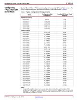
Configuring FPGAs from SPI Serial Flash Configuring FPGAs from SPI Serial Flash Spartan-3E and Virtex-5 FPGAs can be configured from a single SPI serial flash memory. The typical configuration density requirements for these FPGAs are provided in Table 2. Table 2: Typical Configuration Bit Requirements Configuration Bits (Per Device) Smallest SPI Serial Flash Required A larger SPI serial flash device can be used for daisy-chained applications, storing multiple FPGA configuration bitstreams, or for applications storing additional user data, such as code for the embedded MicroBlaze™ or PowerPC™...
Open the catalog to page 3
Configuring FPGAs from SPI Serial Flash A detailed SPI configuration setup is shown in Figure 2, page 5, where the Virtex-5 FPGA is the master and the Numonyx SPI serial flash is the slave. The configuration connections from the SPI serial flash to the FPGA are highlighted in this diagram. For information on the programming and configuration headers used by the Xilinx cables, refer to Hardware and Connections for SPI Programming. A detailed SPI configuration setup is shown in Figure 3, page 6, where the Spartan-3E FPGA is the master and the Numonyx SPI serial flash is the slave. The configuration...
Open the catalog to page 4
Configuring FPGAs from SPI Serial Flash X-Ref Target - Figure 2 Ribbon Cable Header for FPGA JTAG Configuration Ribbon Cable Header for SPI Direct Programming(6) INIT_B DONE SPI Variant ‘1’ ‘0’ Select (Read 0X03) '1' VCCO_2 supplies the SPI configuration dual-mode pins: MOSI, FCS_B, and FS[2:0] VCC_CONFIG (Vcco_0) is the configuration output supply voltage and supplies the dedicated configuration pins: TMS, TCK, TDO, TDI, M[2:0], HSWAPEN, PROG_B, DONE, INIT_B, CCLK, D_IN. PROG_B should be held Low during the direct programming of the SPI serial flash. PROG_B can be driven Low to High with external...
Open the catalog to page 5All Trenz Electronic GmbH catalogs and technical brochures
 Digilent Inc
17 Pages
 EMC2 -DP
2 Pages
 Platform Cable USB
20 Pages
- Connector
- Power supply unit
- Data connector
- Rectangular housing
- Metal box
- Single-output power supply
- Male connector
- Cable connector
- Ethernet PC
- Compact power supply
- Aluminium housing
- Custom housing
- Transceiver module
- Compact housing
- Data acquisition unit
- Plug connector
- AC/AC power supply
- Fiber optics connector
- Processor
- Manufacturing enclosure