- Catalogs
- TOPWAY LCD
- SOLOMON SYSTECH SSD1963 LCD Display Controller
- Company
- Products
- Catalogs
- News & Trends
- Exhibitions
SOLOMON SYSTECH SSD1963 LCD Display Controller
1 /93Pages

SOLOMON SYSTECH SSD1963 LCD Display Controller
1 /93Pages
Catalog excerpts

SOLOMON SYSTECH SEMICONDUCTOR TECHNICAL DATA Advance Information 1215KB Embedded Display SRAM LCD Display Controller This document contains information on a new product. Specifications and information herein are subject to change without notice. http://www.solomon-systech.com SSD1963 Rev 1.1 P 1/93 Copyright © 2010 Solomon Systech Limited
Open the catalog to page 1
Appendix: IC Revision history of SSD1963 Specification Version 0.10 21-Nov-08 0.10 08-Dec-08 Change Items Changed status to Advance Information Update min/max rating of VDDD and VDDPLL in Table 11-1 Added tape and reel drawing of 128-pin LQFP package in Section 15.3 Revised Section 13.2 5. Added 12 bits for Table 7-1 Removed TTL interface Revised section 7.1.5 Change the title of section 7.2 Revised command description in section 8 Removed the command 0x0C and 0x3A Added figures in section 13.4 Revised figures in section 13.3 Revise Table 6-1 Update Table 7-1 Revised section 9.72 Solomon Systech...
Open the catalog to page 2
Solomon Systech
Open the catalog to page 3
Solomon Systech
Open the catalog to page 4
Solomon Systech
Open the catalog to page 5
Solomon Systech
Open the catalog to page 6
Solomon Systec
Open the catalog to page 7
GENERAL DESCRIPTION SSD1963 is a display controller of 1215K byte frame buffer to support up to 864 x 480 x 24bit graphics content. It also equips parallel MCU interfaces in different bus width to receive graphics data and command from MCU. Its display interface supports common RAM-less LCD driver of color depth up to 24 bit-perpixel. Display feature − Built-in 1215K bytes frame buffer. Support up to 864 x 480 at 24bpp display − Support TFT 18/24-bit generic RGB interface panel − Support 8-bit serial RGB interface − Hardware rotation of 0, 90, 180, 270 degree − Hardware display mirroring − Hardware...
Open the catalog to page 8
BLOCK DIAGRAM Figure 4-1: SSD1963 Block Diagram Solomon Systech
Open the catalog to page 9
80 balls TFBGA Figure 5-1: Pinout Diagram –TFBGA (Topview) Solomon Systech Signal Name LDATA4 LDATA3 LDATA2 LDATA1 VSS VDDD R/W# (WR#) D[4] VDDPLL LDATA18 LDATA19 LDATA0 D[19] VSS VDDD E(RD#) D[3] CLK
Open the catalog to page 10
Figure 5-2 : Pinout Diagram – LQFP (Topview) Solomon Systech
Open the catalog to page 11
Signal Name VDDD VSS VSS VDDIO VSS VDDD D0 D1 D2 D3 D4 VDDIO VSS VDDD CLK VDDIO VSS VDDPLL VSSPLL VSS VDDD XTAL_IN VSS XTAL_OUT VDDD VSS VDDLCD LDATA23 LDATA22 LDATA21 LDATA20 VDDD Solomon Systech Signal Name VSS VDDLCD LDATA17 GPIO0 GPIO1 GPIO2 GPIO3 VDDD VSS VDDLCD LFRAME LLINE LSHIFT VDDD VSS VDDLCD LDEN TE PWM GAMAS0 GAMAS1 VDDLCD VSS VDDD VSS VDDLCD LDATA16 LDATA15 LDATA14 LDATA13 LDATA12 VDDD Signal Name VDDIO D17 D16 VDDIO VSS VDDD D15 D14 D13 D12 D11 VDDIO VSS VDDD D10 D9 D8 D7 D6 D5 VDDIO VSS VDDD R/W#(WR#) E(RD#) D/C# CS# VDDIO VSS VDDD RESET# CONF
Open the catalog to page 12
Key: I = Input O =Output IO = Bi-directional (input/output) P = Power pin Hi-Z = High impedance Table 6-1: MCU Interface Pin Mapping Pin Name Reference Type Voltage Level VDDIO VDDIO Description TTL clock input. This pin should be tied to VSS if TTL clock input is not used Crystal oscillator input. This pin should be tied to VSS if not used Crystal oscillator output. This pin should be floating if not used Chip select Data/Command select 6800 mode: E (enable signal) 8080 mode: RD# (read strobe signal) 6800 mode: R/W# 0: Write cycle 1: Read cycle 8080 mode: WR# (write strobe signal) Solomon Systech...
Open the catalog to page 13
Table 6-2: LCD Interface Pin Mapping Pin Name LFRAME LLINE LSHIFT LDEN Reference Type Voltage Level O VDDLCD O VDDLCD O VDDLCD O VDDLCD VDDLCD VDDLCD Description Vertical sync (Frame pulse) Horizontal sync (Line pulse) Pixel clock (Pixel shift signal) Data valid These pins can be configured for display 36, 37, 38, 39 miscellaneous signals or as general purpose I/O. Default as input 52, 53 Gamma selection for panel 51 PWM output for backlight driver Table 6-3: Control Signal Pin Mapping Pin Name RESET# CONF Reference Type Voltage Level I VDDIO I Description Master synchronize reset MCU interface...
Open the catalog to page 14
Note (1) These pin mappings use signal names commonly used for each panel type, however signal names may differ between panel manufacturers. Solomon Systech
Open the catalog to page 15
FUNCTIONAL BLOCK DESCRIPTIONS The MCU interface connects the MCU and SSD1963 graphics controller. The MCU interface can be configured as 6800 mode and 8080 mode by the CONF pin. By pulling the CONF pin to VSSIO, the MCU interface will be configured as 6800 mode interface. If the CONF pin is connected to VDDIO, the MCU interface will be configure in 8080 mode. The 6800 mode MCU interface consist of CS#, D/C#, E, R/W#, D[23:0], and TE signals (Please refer to Table 6-1 for pin multiplexed with 8080 mode). This interface supports both fixed E and clock E scheme to define a read/write cycle. If the...
Open the catalog to page 16
Table 7-1: Pixel Data Format Tearing Effect Signal (TE) The Tearing Effect Signal (TE) is a feedback signal from the LCD Controller to MCU. This signal reveals the display status of LCD controller. In the non-display period, the TE signal will go high. Therefore, this signal enables the MCU to send data by observing the non-display period to avoid tearing. Figure 7-1 shows how the TE signal helps to avoid tearing. If the MCU writing speed is slower than the display speed, the display data should be updated after the LCD controller start to scan the frame buffer. Then the LCD controller will always...
Open the catalog to page 17
Figure 7-1: Relationship between Tearing Effect Signal and MCU Memory Writing In SSD1963, users can configure the TE signal to reflect the vertical non-display period only or reflect both vertical and horizontal non-display period. With the additional horizontal non-display period information, the MCU can control the refresh action in more accurately by counting the horizontal line scanned by the LCD controller. Usually, a fast MCU will not need horizontal non-display period. But a slow MCU will need it to ensure the frame buffer update process always lags behind the LCD controller. System Clock...
Open the catalog to page 18
Figure 7-2: Clock Control Diagram set_pll bit 1 set_pll bit 0 EXTERNAL CRYSTAL Frame Buffer There are 1215K bytes built-in SRAM inside SSD1963 to use as frame buffer. When the frame buffer is written or read, the “address counter” will automatically increase by one or decrease by one depends on the frame buffer settings. Table 7-2: Frame Buffer Settings regarding to set_address_mode command 0x36 System Clock and Reset Manager The “System Clock and Reset Manager” distributes the reset signal and clock signal to the entire system. It controls the Clock Generator and contains clock gating circuitry...
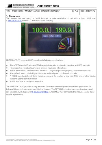
Open the catalog to page 19All TOPWAY LCD catalogs and technical brochures
 TOPWAY Smart LCD SGTools Handbook
108 Pages
 10.1" TFT LCD Module
1 Page
 MONO Product
2 Pages
 LMT050DNCFWU-NNA-2
15 Pages
 LMT080TDGP01
16 Pages
 HKT035BTB-1D
36 Pages
 HMT050AMC-C
17 Pages
 HMT043ATA-6C
31 Pages
 TM035PDHG09
42 Pages
 TM035PDHG03
31 Pages
 TM028HDZP01
28 Pages
 LM256160DCW-1
14 Pages
 LM12896FCW-1
17 Pages
 LM12832KCW
13 Pages
 LM2088EFW-9
12 Pages
 LM3122AGG-2
12 Pages
 LM240160YCW
18 Pages
 LM6093ACW
14 Pages
 HMT104ATA-C
11 Pages
 HMT101ATA-D
36 Pages
 HKT080ATA-C
1 Page
 HMT080ATA
1 Page
 HKT070DTA-1C
11 Pages
 HMT070DTA-D
1 Page
 HKT070DMC-2C
19 Pages
 HMT070ETD-C
31 Pages
 HMT070ETD-1D
34 Pages
 HMT056ATA-C
1 Page
 HMT050CB-1C
31 Pages
 HMT050DTA-D
1 Page
 HKT050ATA-C
1 Page
 HMT043ATA-7C
32 Pages
 HMT043GTA-1D
37 Pages
 HKT043BMC-2C
17 Pages
 HMT043ATA-3C
11 Pages
 HMT043BMC-C
1 Page
 HMT043ATA-4C
11 Pages
 HKT043BMC-C
1 Page
 HKT043ATA-1C
12 Pages
 HMT035ATA-D
13 Pages
 HMT028ATB-C
12 Pages
 HKT104ATA-C
31 Pages
 HMT068BTA-C
33 Pages
 HMT070ATA-1C
32 Pages
 HMT080ATA-C
33 Pages
 HMT090ATA-C
30 Pages
 HMT101ATA-C
33 Pages
 HMT050ATA-2C
31 Pages
 HMT043ATA-2C
32 Pages
 IC Raio RA6963 LCD Controller
42 Pages
 IC Epson S1D13L01 LCD Controller
118 Pages
 IC EPSON S1D13700 LCD Controller
133 Pages
 EPSON S1D13709 LCD Controller
192 Pages
 Samsung S6B0108 LCD Driver
23 Pages
 Avant SBN0064G LCD Driver
37 Pages
 Avant SBN6400G LCD Driver
34 Pages
 EPSON SED1335 LCD Controller
95 Pages
 SGS-THOMSON ST7282
23 Pages
 Raio RA6963 LCD Controller
42 Pages
 Raio RA8875 TFT LCD Controller
174 Pages
 Raio RA8835 LCD Controller
93 Pages
 RAIO RA8803 LCD Controller
8 Pages
 HMT035ATA-1C
1 Page
 Smart LCD introduction
14 Pages
 Topway company introduction
14 Pages
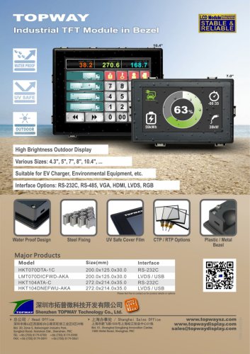 TFT module in bezel
1 Page
 Topway TFT LCD
1 Page
 LM12864L Series
1 Page
 LM12864T Series
1 Page
 LM12864F Series
1 Page
 LM6060C Series
1 Page
 LM12864M Series
1 Page
 LM6029A Series
1 Page
 LM6059B Series
1 Page
 LM24048A Series
1 Page
 LM13232A Series
1 Page
 LM160160A Series
1 Page
 LMB402C Series
1 Page
 LMB242A Series
1 Page
 LMB204C Series
1 Page
 LM3121 Series
1 Page
 LMB404A Series
1 Page
 HMT043FC-1C
1 Page
 LM3123 Series
1 Page
 LMB204B Series
1 Page
 LMB202E Series
1 Page
 LMB202D Series
1 Page
 LMB164A Series
1 Page
 LMB162G Series
1 Page
 LMB162H Series
1 Page
 LMB162N Series
1 Page
 LMB162A Series
1 Page
 LMB0820D Series
1 Page
 LMB0820C Series
1 Page
 LMB0820A Series
1 Page
 LMB081N Series
1 Page
 LMB081A Series
1 Page
 LMB162X series
1 Page
 LMT057DNAFWU-AAN series
1 Page
 LMT057DNAFWU-AAA series
1 Page
 LMT104SDH01 Series
1 Page
 TOPWAY Product List (Y2012)
4 Pages
 TFT LCD module
1 Page
 Without controller
1 Page
 Chinese fonts
1 Page
 Built-in controller
1 Page
 Character module
1 Page


- Monitor with touchscreen
- Industrial monitor
- HDMI monitor
- VESA mounting monitor
- Industrial display panel
- TFT display module
- IP65 monitor
- Touch screen display panel
- Color display panel
- LED display panel
- High-brightness monitor
- TFT-LCD monitor
- Electronic display panel
- Control display system
- Wall-mount monitor
- IPS display panel
- Backlit display panel
- Programmable display system