- Catalogs
- TOPWAY LCD
- Samsung S6B0108 LCD Driver
- Company
- Products
- Catalogs
- News & Trends
- Exhibitions
Samsung S6B0108 LCD Driver
1 /23Pages

Samsung S6B0108 LCD Driver
1 /23Pages
Catalog excerpts

64 CH SEGMENT DRIVER FOR DOT MATRIX LCD Contents in this document are subject to change without notice. No part of this document may be reproduced or transmitted in any form or by any means, electronic or mechanical, for any purpose, without the express written permission of LCD Driver IC Team.
Open the catalog to page 1
64CH SEGMENT DRIVER FOR DOT MATRIX LCD INTRODUCTION The S6B0108 is a LCD driver LSI with 64 channel output for dot matrix liquid crystal graphic display systems. This device consists of the display RAM, 64 bit data latch, 64 bit drivers and decoder logic. It has the internal display RAM for storing the display data transferred from a 8 bit micro controller and generates the dot matrix Iiquid crystal driving signals corresponding to stored data. The S6B0108 composed of the liquid crystal display system in combination with the S6B0107 (64 channel common driver). Dot matrix LCD segment driver with...
Open the catalog to page 2
64CH SEGMENT DRIVER FOR DOT MATRIX LCD Output Register Display On/Off Input Register BLOCK DIAGRAM Instruction Decoder Page Selector Display Start Line Register
Open the catalog to page 3
64CH SEGMENT DRIVER FOR DOT MATRIX LCD Chip size: 4090 × 4020 PAD size: 100 × 100 Unit : µm There is mark of S6B0108 on the bottom left in the chip.
Open the catalog to page 4
64CH SEGMENT DRIVER FOR DOT MATRIX LCD PAD CENTER COORDINATES PAD Number
Open the catalog to page 5
64CH SEGMENT DRIVER FOR DOT MATRIX LCD PIN DESCRIPTION Table 1. Pin Description Pin Number QFP(TQFP) 3(1) 78(76) 73(71), 8(6) Input / Output Description For internal logic circuit (+5V ± 10%) GND (0V) For LCD driver circuit VSS = 0V, VDD = +5V ± 10%, VDD-VEE = 8V - 17V VEE1 and VEE2 is connected by the same voltage. Bias supply voltage terminals to drive the LCD. Chip selection In order to interface data for input or output, the terminals have to be CS1B = L, CS2B = L, and CS3 = H. Alternating signal input for LCD driving. Address control signal to determine the relation between Y address of...
Open the catalog to page 6
64CH SEGMENT DRIVER FOR DOT MATRIX LCD Table 1. Pin Description (Continued) Pin Number QFP(TQFP) Input / Output Description Read or Write. R/W = H → Data appears at DB<0:7> and can be read by the CPU while E = H, CS1B = L, CS2B = L and CS3 = H . R/W = L → Display data DB<0:7> can be written at falling of E when CS1B = L, CS2B = L and CS3 = H. Data bus. Three state I/O common terminal. LCD segment driver output. Display RAM data 1: On Display RAM data 0: Off (relation of display RAM data & M) Reset signal. When RSTB=L, 93(91) - ON / OFF register becomes set by 0. (display off) – Display start...
Open the catalog to page 7
64CH SEGMENT DRIVER FOR DOT MATRIX LCD MAXIMUM ABSOLUTE LIMIT Characteristic Operating voltage Supply voltage Operating temperature Storage temperature Driver supply voltage NOTES: 1. Based on VSS = 0V. 2. Applies the same supply voltage to VEE1 and VEE2. VLCD=VDD-VEE. 3. 4. Applies to M, FRM, CL, RSTB, ADC, CLK1, CLK2, CS1B, CS2B, CS3, E, R/W, RS and DB0 - DB7. Applies to V0L(R), V2L(R), V3L(R) and V5L(R). Voltage level: VDD ≥ V0L = V0R ≥ V2L = V2R ≥ V3L = V3R ≥ V5L = V5R
Open the catalog to page 8
64CH SEGMENT DRIVER FOR DOT MATRIX LCD ELECTRICAL CHARACTERISTICS DC CHARACTERISTICS (VDD = +5V ± 10%, VSS = 0V, VDD-VEE = 8 to 17V, Ta =-30 to +85° C) ° Characteristic Input high voltage Output high voltage Input leakage current Three-state(off) input current Driver input leakage current During display During access Access cycle = 1MHz Operating current NOTES: 1. CL, FRM, M RSTB, CLK1, CLK2 2. CS1B, CS2B, CS3, E, R/W, RS, DB0 - DB7 3. DB0 - DB7 4. Except DB0 - DB7 5. DB0 - DB7 at high impedance 6. V0L(R), V2L(R), V3L(R), V5L(R) 7. 1/64 duty, FCLK = 250kHz, frame frequency = 70HZ, output: no...
Open the catalog to page 9
64CH SEGMENT DRIVER FOR DOT MATRIX LCD AC CHARACTERISTICS (VDD = +5V ± 10%, VSS = 0V, Ta =-30 to +85° C) ° Clock Timing Characteristic CLK1 "high" level width CLK2 "high" level width Figure 1. External Clock Waveform
Open the catalog to page 10
64CH SEGMENT DRIVER FOR DOT MATRIX LCD Display Control Timing Characteristic CL "high" level width Figure 2. Display Control Waveform
Open the catalog to page 11
64CH SEGMENT DRIVER FOR DOT MATRIX LCD E high level width Address set-up time Address hold time Data set-up time Data delay time Data hold time (write) Data hold time (read) Figure 3. MPU Write Timing
Open the catalog to page 12
64CH SEGMENT DRIVER FOR DOT MATRIX LCD Figure 4. MPU Read Timing
Open the catalog to page 13
64CH SEGMENT DRIVER FOR DOT MATRIX LCD OPERATING PRINCIPLES AND METHODS I/O BUFFER Input buffer controls the status between the enable and disable of chip. Unless the CS1B to CS3 is in active mode, Input or output of data and instruction does not execute. Therefore internal state is not change. But RSTB and ADC can operate regardless CS1B-CS3. INPUT REGISTER Input register is provided to interface with MPU which is different operating frequency. Input register stores the data temporarily before writing it into display RAM. When CS1B to CS3 are in the active mode, R/W and RS select the input register....
Open the catalog to page 14
64CH SEGMENT DRIVER FOR DOT MATRIX LCD RESET The system can be initialized by setting RSTB terminal at low level when turning power on, receiving instruction from MPU. When RSTB becomes low, following procedure is occurred. • Display start line register become set by 0. (Z-address 0) While RSTB is low, No instruction except status read can be accepted. Therefore, execute other instructions after making sure that DB4 = 0 (clear RSTB) and DB7 = 0 (ready) by status read instruction. The Conditions of power supply at initial power up are shown in table 1. Table 2. Power Supply Initial Conditions...
Open the catalog to page 15
64CH SEGMENT DRIVER FOR DOT MATRIX LCD Busy Flag Busy Flag indicates that S6B0108 is operating or no operating. When busy flag is high, S6B0108 is in internal operating. When busy flag is low, S6B0108 can accept the data or instruction. DB7 indicates busy flag of the S6B0108. Data at address N Busy check Busy check Read data Busy (dummy) check Read data Busy at address check N Data read address N + 1 Busy Check E Busy Flag T Busy fCLK is CLK1, CLK2 frequency Busy Flag
Open the catalog to page 16All TOPWAY LCD catalogs and technical brochures
 TOPWAY Smart LCD SGTools Handbook
108 Pages
 10.1" TFT LCD Module
1 Page
 MONO Product
2 Pages
 LMT050DNCFWU-NNA-2
15 Pages
 LMT080TDGP01
16 Pages
 HKT035BTB-1D
36 Pages
 HMT050AMC-C
17 Pages
 HMT043ATA-6C
31 Pages
 TM035PDHG09
42 Pages
 TM035PDHG03
31 Pages
 TM028HDZP01
28 Pages
 LM256160DCW-1
14 Pages
 LM12896FCW-1
17 Pages
 LM12832KCW
13 Pages
 LM2088EFW-9
12 Pages
 LM3122AGG-2
12 Pages
 LM240160YCW
18 Pages
 LM6093ACW
14 Pages
 HMT104ATA-C
11 Pages
 HMT101ATA-D
36 Pages
 HKT080ATA-C
1 Page
 HMT080ATA
1 Page
 HKT070DTA-1C
11 Pages
 HMT070DTA-D
1 Page
 HKT070DMC-2C
19 Pages
 HMT070ETD-C
31 Pages
 HMT070ETD-1D
34 Pages
 HMT056ATA-C
1 Page
 HMT050CB-1C
31 Pages
 HMT050DTA-D
1 Page
 HKT050ATA-C
1 Page
 HMT043ATA-7C
32 Pages
 HMT043GTA-1D
37 Pages
 HKT043BMC-2C
17 Pages
 HMT043ATA-3C
11 Pages
 HMT043BMC-C
1 Page
 HMT043ATA-4C
11 Pages
 HKT043BMC-C
1 Page
 HKT043ATA-1C
12 Pages
 HMT035ATA-D
13 Pages
 HMT028ATB-C
12 Pages
 HKT104ATA-C
31 Pages
 HMT068BTA-C
33 Pages
 HMT070ATA-1C
32 Pages
 HMT080ATA-C
33 Pages
 HMT090ATA-C
30 Pages
 HMT101ATA-C
33 Pages
 HMT050ATA-2C
31 Pages
 HMT043ATA-2C
32 Pages
 IC Raio RA6963 LCD Controller
42 Pages
 IC Epson S1D13L01 LCD Controller
118 Pages
 IC EPSON S1D13700 LCD Controller
133 Pages
 EPSON S1D13709 LCD Controller
192 Pages
 Avant SBN0064G LCD Driver
37 Pages
 Avant SBN6400G LCD Driver
34 Pages
 EPSON SED1335 LCD Controller
95 Pages
 SGS-THOMSON ST7282
23 Pages
 Raio RA6963 LCD Controller
42 Pages
 Raio RA8875 TFT LCD Controller
174 Pages
 Raio RA8835 LCD Controller
93 Pages
 RAIO RA8803 LCD Controller
8 Pages
 HMT035ATA-1C
1 Page
 Smart LCD introduction
14 Pages
 Topway company introduction
14 Pages
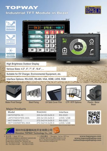 TFT module in bezel
1 Page
 Topway TFT LCD
1 Page
 LM12864L Series
1 Page
 LM12864T Series
1 Page
 LM12864F Series
1 Page
 LM6060C Series
1 Page
 LM12864M Series
1 Page
 LM6029A Series
1 Page
 LM6059B Series
1 Page
 LM24048A Series
1 Page
 LM13232A Series
1 Page
 LM160160A Series
1 Page
 LMB402C Series
1 Page
 LMB242A Series
1 Page
 LMB204C Series
1 Page
 LM3121 Series
1 Page
 LMB404A Series
1 Page
 HMT043FC-1C
1 Page
 LM3123 Series
1 Page
 LMB204B Series
1 Page
 LMB202E Series
1 Page
 LMB202D Series
1 Page
 LMB164A Series
1 Page
 LMB162G Series
1 Page
 LMB162H Series
1 Page
 LMB162N Series
1 Page
 LMB162A Series
1 Page
 LMB0820D Series
1 Page
 LMB0820C Series
1 Page
 LMB0820A Series
1 Page
 LMB081N Series
1 Page
 LMB081A Series
1 Page
 LMB162X series
1 Page
 LMT057DNAFWU-AAN series
1 Page
 LMT057DNAFWU-AAA series
1 Page
 LMT104SDH01 Series
1 Page
 TOPWAY Product List (Y2012)
4 Pages
 TFT LCD module
1 Page
 Without controller
1 Page
 Chinese fonts
1 Page
 Built-in controller
1 Page
 Character module
1 Page


- Monitor with touchscreen
- Industrial monitor
- LCD display panel
- HDMI monitor
- VESA mounting monitor
- Industrial display panel
- TFT display module
- IP65 monitor
- Touch screen display panel
- Color display panel
- LED display panel
- High-brightness monitor
- TFT-LCD monitor
- Electronic display panel
- Control display system
- Wall-mount monitor
- IPS display panel
- Backlit display panel
- Programmable display system