- Catalogs
- TOPWAY LCD
- S1D13705 Embedded Memory LCD Controller
- Company
- Products
- Catalogs
- News & Trends
- Exhibitions
S1D13705 Embedded Memory LCD Controller
1 /480Pages

S1D13705 Embedded Memory LCD Controller
1 /480Pages
Catalog excerpts

S1D13705 Embedded Memory LCD Controller Copyright © 2001 Epson Research and Development, Inc. All Rights Reserved. Information in this document is subject to change without notice.You may download and use this document, but only for your own use in evaluating Seiko Epson/EPSON products. You may not modify the document. Epson Research and Development, Inc. disclaims any representation that the contents of this document are accurate or current. The Programs/Technologies described in this document may contain material protected under U.S. and/or International Patent laws. EPSON is a registered trademark of Seiko Epson Corporation. All other Trademarks are the property of their respective owners
Open the catalog to page 1
Epson Research and Development Vancouver Design Center THIS PAGE LEFT BLANK TECHNICAL MANUAL Issue Date: 01/04/18
Open the catalog to page 2
Epson Research and Development Vancouver Design Center Customer Support Information Comprehensive Support Tools Seiko Epson Corp. provides to the system designer and computer OEM manufacturer a complete set of resources and tools for the development of graphics systems. Evaluation / Demonstration Board • Assembled and fully tested graphics evaluation board with installation guide and schematics. • To borrow an evaluation board, please contact your local Seiko Epson Corp. sales representative. Chip Documentation • Technical manual includes Data Sheet, Application Notes, and Programmer’s Reference....
Open the catalog to page 3
Epson Research and Development Vancouver Design Center THIS PAGE LEFT BLANK TECHNICAL MANUAL Issue Date: 01/04/18
Open the catalog to page 4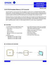
S1D13705 Embedded Memory LCD Controller The S1D13705 is a color/monochrome LCD graphics controller with an embedded 80K Byte SRAM display buffer. The high integration of the S1D13705 provides a low cost, low power, single chip solution to meet the requirements of embedded markets such as Office Automation equipment, Mobile Communications devices, and Palm-size PCs where board size and battery life are major concerns. Products requiring a “Portrait” display can take advantage of the Hardware Portrait Mode feature of the S1D13705. Virtual and Split Screen are just some of the display modes supported....
Open the catalog to page 5
GRAPHICS S1D13705 ■ DESCRIPTION Memory Interface • Embedded 80K byte SRAM display buffer. CPU Interface • Direct support for: Hitachi SH-3. Hitachi SH-4. Motorola M68xxx. MPU bus interface with programmable READY. • CPU write buffer. Display Support • 4/8-bit monochrome LCD interface. • Single-panel, single-drive passive displays. • Dual-panel, dual-drive passive displays. • Active matrix TFT / D-TFD interface. • Example resolutions: 640x480 at a color depth of 2 bpp. 640x240 at a color depth of 4 bpp. 320x240 at a color depth of 8 bpp. Clock Source • Single clock input for both pixel and memory...
Open the catalog to page 6
S1D13705 Embedded Memory LCD Controller Hardware Functional Specification Document Number: X27A-A-001-09 Copyright © 1999, 2001 Epson Research and Development, Inc. All Rights Reserved. Information in this document is subject to change without notice.You may download and use this document, but only for your own use in evaluating Seiko Epson/EPSON products. You may not modify the document. Epson Research and Development, Inc. disclaims any representation that the contents of this document are accurate or current. The Programs/Technologies described in this document may contain material protected...
Open the catalog to page 7
Epson Research and Development Vancouver Design Center THIS PAGE LEFT BLANK Hardware Functional Specification Issue Date: 01/05/22
Open the catalog to page 8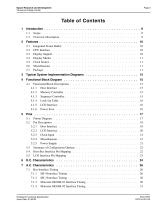
Epson Research and Development Vancouver Design Center Features . . . . . . . . . . 2.1 Integrated Frame Buffer 2.2 CPU Interface . . . . 2.3 Display Support . . . . 2.4 Display Modes . . . . 2.5 Clock Source . . . . . 2.6 Miscellaneous . . . . 2.7 Package . . . . . . . Typical System Implementation Diagrams . . . . . . . . . . . . . . . . . . . . . . 12 Functional Block Diagram . . . . . 4.1 Functional Block Descriptions . . 4.1.1 Host Interface . . . . . . . . 4.1.2 Memory Controller . . . . . 4.1.3 Sequence Controller . . . . . 4.1.4 Look-Up Table . . . . . . . 4.1.5 LCD Interface . . . ....
Open the catalog to page 9
Epson Research and Development Vancouver Design Center 7.1.5 Generic #1 Interface Timing . . . . . . . . . . . 7.1.6 Generic #2 Interface Timing . . . . . . . . . . . 7.2 Clock Input Requirements . . . . . . . . . . . 7.3 Display Interface . . . . . . . . . . . . . . . 7.3.1 Power On/Reset Timing . . . . . . . . . . . . . 7.3.2 Power Down/Up Timing . . . . . . . . . . . . 7.3.3 Single Monochrome 4-Bit Panel Timing . . . . 7.3.4 Single Monochrome 8-Bit Panel Timing . . . . 7.3.5 Single Color 4-Bit Panel Timing . . . . . . . . 7.3.6 Single Color 8-Bit Panel Timing (Format 1) . . 7.3.7 Single Color...
Open the catalog to page 10
Epson Research and Development Vancouver Design Center List of Tables Table 5-1: Summary of Power On/Reset Options . . . . . . . . . . . . . . . . Table 5-2: Host Bus Interface Pin Mapping . . . . . . . . . . . . . . . . . . . Table 5-3: LCD Interface Pin Mapping . . . . . . . . . . . . . . . . . . . . . Table 6-1: Absolute Maximum Ratings . . . . . . . . . . . . . . . . . . . . . Table 6-2: Recommended Operating Conditions for Core VDD = 3.3V ± 10% Table 6-3: Input Specifications . . . . . . . . . . . . . . . . . . . . . . . . . Table 6-4: Output Specifications. . . . . . . . . . . . . . . ....
Open the catalog to page 11
Epson Research and Development Vancouver Design Center THIS PAGE LEFT BLANK Hardware Functional Specification Issue Date: 01/05/22
Open the catalog to page 12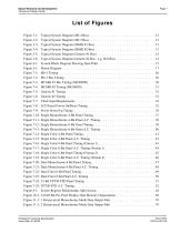
Epson Research and Development Vancouver Design Center List of Figures Figure 3-1: Figure 3-2: Figure 3-3: Figure 3-4: Figure 3-5: Figure 3-6: Figure 4-1: Figure 5-1: Figure 7-1: Figure 7-2: Figure 7-3: Figure 7-4: Figure 7-5: Figure 7-6: Figure 7-7: Figure 7-8: Figure 7-9: Figure 7-10: Figure 7-11: Figure 7-12: Figure 7-13: Figure 7-14: Figure 7-15: Figure 7-16: Figure 7-17: Figure 7-18: Figure 7-19: Figure 7-20: Figure 7-21: Figure 7-22: Figure 7-23: Figure 7-24: Figure 7-25: Figure 8-1: Figure 10-1: Figure 11-1: Figure 11-2: Typical System Diagram (SH-4 Bus). . . . . . . . . . . . . . . ....
Open the catalog to page 13All TOPWAY LCD catalogs and technical brochures
 TOPWAY Smart LCD SGTools Handbook
108 Pages
 10.1" TFT LCD Module
1 Page
 MONO Product
2 Pages
 LMT050DNCFWU-NNA-2
15 Pages
 LMT080TDGP01
16 Pages
 HKT035BTB-1D
36 Pages
 HMT050AMC-C
17 Pages
 HMT043ATA-6C
31 Pages
 TM035PDHG09
42 Pages
 TM035PDHG03
31 Pages
 TM028HDZP01
28 Pages
 LM256160DCW-1
14 Pages
 LM12896FCW-1
17 Pages
 LM12832KCW
13 Pages
 LM2088EFW-9
12 Pages
 LM3122AGG-2
12 Pages
 LM240160YCW
18 Pages
 LM6093ACW
14 Pages
 HMT104ATA-C
11 Pages
 HMT101ATA-D
36 Pages
 HKT080ATA-C
1 Page
 HMT080ATA
1 Page
 HKT070DTA-1C
11 Pages
 HMT070DTA-D
1 Page
 HKT070DMC-2C
19 Pages
 HMT070ETD-C
31 Pages
 HMT070ETD-1D
34 Pages
 HMT056ATA-C
1 Page
 HMT050CB-1C
31 Pages
 HMT050DTA-D
1 Page
 HKT050ATA-C
1 Page
 HMT043ATA-7C
32 Pages
 HMT043GTA-1D
37 Pages
 HKT043BMC-2C
17 Pages
 HMT043ATA-3C
11 Pages
 HMT043BMC-C
1 Page
 HMT043ATA-4C
11 Pages
 HKT043BMC-C
1 Page
 HKT043ATA-1C
12 Pages
 HMT035ATA-D
13 Pages
 HMT028ATB-C
12 Pages
 HKT104ATA-C
31 Pages
 HMT068BTA-C
33 Pages
 HMT070ATA-1C
32 Pages
 HMT080ATA-C
33 Pages
 HMT090ATA-C
30 Pages
 HMT101ATA-C
33 Pages
 HMT050ATA-2C
31 Pages
 HMT043ATA-2C
32 Pages
 IC Raio RA6963 LCD Controller
42 Pages
 IC Epson S1D13L01 LCD Controller
118 Pages
 IC EPSON S1D13700 LCD Controller
133 Pages
 EPSON S1D13709 LCD Controller
192 Pages
 Samsung S6B0108 LCD Driver
23 Pages
 Avant SBN0064G LCD Driver
37 Pages
 Avant SBN6400G LCD Driver
34 Pages
 EPSON SED1335 LCD Controller
95 Pages
 SGS-THOMSON ST7282
23 Pages
 Raio RA6963 LCD Controller
42 Pages
 Raio RA8875 TFT LCD Controller
174 Pages
 Raio RA8835 LCD Controller
93 Pages
 RAIO RA8803 LCD Controller
8 Pages
 HMT035ATA-1C
1 Page
 Smart LCD introduction
14 Pages
 Topway company introduction
14 Pages
 TFT module in bezel
1 Page
 Topway TFT LCD
1 Page
 LM12864L Series
1 Page
 LM12864T Series
1 Page
 LM12864F Series
1 Page
 LM6060C Series
1 Page
 LM12864M Series
1 Page
 LM6029A Series
1 Page
 LM6059B Series
1 Page
 LM24048A Series
1 Page
 LM13232A Series
1 Page
 LM160160A Series
1 Page
 LMB402C Series
1 Page
 LMB242A Series
1 Page
 LMB204C Series
1 Page
 LM3121 Series
1 Page
 LMB404A Series
1 Page
 HMT043FC-1C
1 Page
 LM3123 Series
1 Page
 LMB204B Series
1 Page
 LMB202E Series
1 Page
 LMB202D Series
1 Page
 LMB164A Series
1 Page
 LMB162G Series
1 Page
 LMB162H Series
1 Page
 LMB162N Series
1 Page
 LMB162A Series
1 Page
 LMB0820D Series
1 Page
 LMB0820C Series
1 Page
 LMB0820A Series
1 Page
 LMB081N Series
1 Page
 LMB081A Series
1 Page
 LMB162X series
1 Page
 LMT057DNAFWU-AAN series
1 Page
 LMT057DNAFWU-AAA series
1 Page
 LMT104SDH01 Series
1 Page
 TOPWAY Product List (Y2012)
4 Pages
 TFT LCD module
1 Page
 Without controller
1 Page
 Chinese fonts
1 Page
 Built-in controller
1 Page
 Character module
1 Page


- Monitor with touchscreen
- Industrial monitor
- LCD display panel
- HDMI monitor
- VESA mounting monitor
- Industrial display panel
- TFT display module
- IP65 monitor
- Touch screen display panel
- Color display panel
- LED display panel
- High-brightness monitor
- TFT-LCD monitor
- Electronic display panel
- Control display system
- Wall-mount monitor
- IPS display panel
- Backlit display panel
- Programmable display system