- Catalogs
- TOPWAY LCD
- LM12896FCW-1
- Company
- Products
- Catalogs
- News & Trends
- Exhibitions
LM12896FCW-1
1 /17Pages

LM12896FCW-1
1 /17Pages
Catalog excerpts

LM12896FCW-1 LCD Module User Manual Release Date Prelimiay release Document Name: LM12896FCW-1-Manual-Rev0.1.doc Page: 1 of 17
Open the catalog to page 1
LCD Module User Manual Table of Content 1. Basic Specifications 2. Absolute Maximum Ratings 3.2 LED Backlight Circuit Characteristics Document Name: LM12896FCW-1-Manual-Rev0.1.doc Page: 2 of 17
Open the catalog to page 2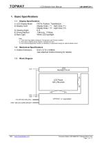
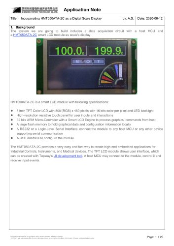
LCD Module User Manual 1. Basic Specifications 1.1 Display Specifications 1) LCD Display Mode : FSTN, Positive, Transflective 2) Display Color : Display Data = “1” : Dark Gray (*1) : Display Data = “0” : Light Gray (*2) 3) Viewing Angle :6H 4) Driving Method : 1/96 duty, 1/10bias 5) Back Light : White LED backlight Note: *1. Color tone may slightly change by Temperature and Driving Condition. *2. The Color is defined as the inactive / background color *3. Fine Contrast adjustment function is necessary in application design for optimal display result 1.2 Mechanical Specifications 1) Outline Dimension...
Open the catalog to page 3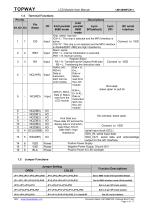
LCD Module User Manual Terminal Functions Descriptions Chip select input pin. /CS=“L”: This chip is selected and the MPU interface is active. Connect to VSS /CS=“H”: This chip is not selected and the MPU interface is disabled(DB7~DB0] are high impedance). Reset signal. /RST = L, internal Initialization is executed. /RST = H, Normal running. Register Select RS = H, Transferring the Display RAM data Connect to VDD RS = L, Transferring the Instruction data /WR=LH, R/W = H, /RD=H; E=L; Data or Data or Instruction Status latch into the read form LCD module the LCD module Not used, leave open or pull...
Open the catalog to page 4
LCD Module User Manual 2. Absolute Maximum Ratings Items Supply Voltage Operating Temperature Storage Temperature Condition VSS = 0V No Condensation No Condensation Cautions: Any Stresses exceeding the Absolute Maximum Ratings may cause substantial damage to the device. Functional operation of this device at other conditions beyond those listed in the specification is not implied and prolonged exposure to extreme conditions may affect device reliability. Items Operating Voltage Input High Voltage Input Low Voltage Output High Voltage Output Low Voltage Operating Current 3.2 VSS = 0V, VDD = 3.3V,...
Open the catalog to page 5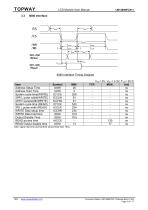
LCD Module User Manual 8080 Interface Timing Diagram Item Address Setup Time Address Hold Time System cycle time(WRITE) /WR L pulse width(WRITE) /WR H pulsewidth(WRITE) System cycle time (READ) /RD L pulse width (READ) WRITE Data setup time WRITE Data hold time Output Disable Time READ access time READ Output disable time note: signal rise time and fall time should less than 15ns. Document Name: LM12896FCW-1-Manual-Rev0.1.doc Page: 6 of 17
Open the catalog to page 6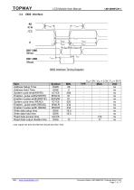
LCD Module User Manual 6800 Interface Timing Diagram Item Address Setup Time Address Hold Time System cycle time(WRITE) Enable L pulse width(WRITE) Enable H pulse width(WRITE) System cycle time (READ) Enable L pulse width (READ) Enable H pulse width (READ) Write data setup time Write data hold time Read data access time Read data output disable time note: signal rise time and fall time should less than 15ns. Document Name: LM12896FCW-1-Manual-Rev0.1.doc Page: 7 of 17
Open the catalog to page 7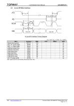
LCD Module User Manual 4-Line SPI Interface Timing Diagram Item Serial clock period SCL “H” pulse width SCL “L” pulse width Address setup time Address hold time Data setup time Data hold time CSB-SCLK time CSB-SCLK time CS “H” pulse width Symbol tSCYC tSHW tSLW tSAS tSAH tSDS tSDH tCSS tCSH tCHW note: signal rise time and fall time should less than 15ns
Open the catalog to page 8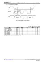
LCD Module User Manual 3-Line SPI Interface Timing Diagram Item Serial clock period SCL “H” pulse width SCL “L” pulse width Data setup time Data hold time CSB-SCL time CSB-SCL time Symbol tSCYC tSHW tSLW tSDS tSDH tCSS tCSH note: signal rise time and fall time should less than 15ns Document Name: LM12896FCW-1-Manual-Rev0.1.doc Page:
Open the catalog to page 9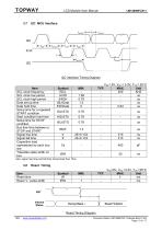
LCD Module User Manual I2C Interface Timing Diagram Item SCL clock frequency SCL clock low period SCL clock high period Data set-up time Data hold time Setup time for a repeated START condition Start condition hold time Setup time for STOP condition Bus free time between a STOP and START Signal rise time Signal fall time Capacitive load represented by each bus line Tolerable spike width on bus Symbol fSCL tLOW tHIGH tSU;Data tHD;Data note: signal rise time and fall time should less than 15ns Reset Timing Item Reset time Reset “L” pulse width Reset Timing Diagram URL: Document Name: LM12896FCW-1-Manual-Rev0.1.doc...
Open the catalog to page 10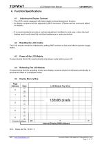
LCD Module User Manual 4. Function Specifications 4.1 Adjusting the Display Contrast -- This LCD module equipped with latest digital contrast adjustment function. -- Its display contrast could be adjusted by MCU command. (Please see the command tables for details) -- It is recommended to provide a contrast adjustment interface for end-user, where the best display result could meet the individual preference in mass production. 4.2 Resetting the LCD module The LCD module should be initialized by setting /RST terminal at low level after the power supply stable. 4.3 Power off the LCD Module It recommends...
Open the catalog to page 11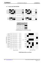
LCD Module User Manual Display Data RAM (DDRAM) Document Name: LM12896FCW-1-Manual-Rev0.1.doc Page: 12 of 17
Open the catalog to page 12
LCD Module User Manual Document Name: LM12896FCW-1-Manual-Rev0.1.doc Page: 13 of 17
Open the catalog to page 13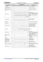
LCD Module User Manual Document Name: LM12896FCW-1-Manual-Rev0.1.doc Page: 14 of 17
Open the catalog to page 14
LCD Module User Manual Document Name: LM12896FCW-1-Manual-Rev0.1.doc Page: 15 of 17
Open the catalog to page 15
LCD Module User Manual *1. Do not use any other command not listed, or the system malfunction may result. *2. For the details of the Display Commands, please refer to ST75161 data sheet. Document Name: LM12896FCW-1-Manual-Rev0.1.doc Page: 16 of 17
Open the catalog to page 16
LCD Module User Manual The LCD panel is made by glass. Any mechanical shock (eg. dropping form high place) will damage the LCD module. Do not add excessive force on the surface of the display, which may cause the Display color change abnormally. The polarizer on the LCD is easily get scratched. If possible, do not remove the LCD protective film until the last step of installation. Never attempt to disassemble or rework the LCD module. Only Clean the LCD with Isopropyl Alcohol or Ethyl Alcohol. Other solvents (eg. water) may damage the LCD. When mounting the LCD module, make sure that it is free...
Open the catalog to page 17All TOPWAY LCD catalogs and technical brochures
 TOPWAY Smart LCD SGTools Handbook
108 Pages
 10.1" TFT LCD Module
1 Page
 MONO Product
2 Pages
 LMT050DNCFWU-NNA-2
15 Pages
 LMT080TDGP01
16 Pages
 HKT035BTB-1D
36 Pages
 HMT050AMC-C
17 Pages
 HMT043ATA-6C
31 Pages
 TM035PDHG09
42 Pages
 TM035PDHG03
31 Pages
 TM028HDZP01
28 Pages
 LM256160DCW-1
14 Pages
 LM12832KCW
13 Pages
 LM2088EFW-9
12 Pages
 LM3122AGG-2
12 Pages
 LM240160YCW
18 Pages
 LM6093ACW
14 Pages
 HMT104ATA-C
11 Pages
 HMT101ATA-D
36 Pages
 HKT080ATA-C
1 Page
 HMT080ATA
1 Page
 HKT070DTA-1C
11 Pages
 HMT070DTA-D
1 Page
 HKT070DMC-2C
19 Pages
 HMT070ETD-C
31 Pages
 HMT070ETD-1D
34 Pages
 HMT056ATA-C
1 Page
 HMT050CB-1C
31 Pages
 HMT050DTA-D
1 Page
 HKT050ATA-C
1 Page
 HMT043ATA-7C
32 Pages
 HMT043GTA-1D
37 Pages
 HKT043BMC-2C
17 Pages
 HMT043ATA-3C
11 Pages
 HMT043BMC-C
1 Page
 HMT043ATA-4C
11 Pages
 HKT043BMC-C
1 Page
 HKT043ATA-1C
12 Pages
 HMT035ATA-D
13 Pages
 HMT028ATB-C
12 Pages
 HKT104ATA-C
31 Pages
 HMT068BTA-C
33 Pages
 HMT070ATA-1C
32 Pages
 HMT080ATA-C
33 Pages
 HMT090ATA-C
30 Pages
 HMT101ATA-C
33 Pages
 HMT050ATA-2C
31 Pages
 HMT043ATA-2C
32 Pages
 IC Raio RA6963 LCD Controller
42 Pages
 IC Epson S1D13L01 LCD Controller
118 Pages
 IC EPSON S1D13700 LCD Controller
133 Pages
 EPSON S1D13709 LCD Controller
192 Pages
 Samsung S6B0108 LCD Driver
23 Pages
 Avant SBN0064G LCD Driver
37 Pages
 Avant SBN6400G LCD Driver
34 Pages
 EPSON SED1335 LCD Controller
95 Pages
 SGS-THOMSON ST7282
23 Pages
 Raio RA6963 LCD Controller
42 Pages
 Raio RA8875 TFT LCD Controller
174 Pages
 Raio RA8835 LCD Controller
93 Pages
 RAIO RA8803 LCD Controller
8 Pages
 HMT035ATA-1C
1 Page
 Smart LCD introduction
14 Pages
 Topway company introduction
14 Pages
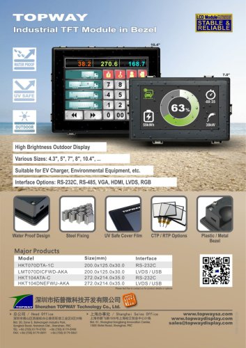 TFT module in bezel
1 Page
 Topway TFT LCD
1 Page
 LM12864L Series
1 Page
 LM12864T Series
1 Page
 LM12864F Series
1 Page
 LM6060C Series
1 Page
 LM12864M Series
1 Page
 LM6029A Series
1 Page
 LM6059B Series
1 Page
 LM24048A Series
1 Page
 LM13232A Series
1 Page
 LM160160A Series
1 Page
 LMB402C Series
1 Page
 LMB242A Series
1 Page
 LMB204C Series
1 Page
 LM3121 Series
1 Page
 LMB404A Series
1 Page
 HMT043FC-1C
1 Page
 LM3123 Series
1 Page
 LMB204B Series
1 Page
 LMB202E Series
1 Page
 LMB202D Series
1 Page
 LMB164A Series
1 Page
 LMB162G Series
1 Page
 LMB162H Series
1 Page
 LMB162N Series
1 Page
 LMB162A Series
1 Page
 LMB0820D Series
1 Page
 LMB0820C Series
1 Page
 LMB0820A Series
1 Page
 LMB081N Series
1 Page
 LMB081A Series
1 Page
 LMB162X series
1 Page
 LMT057DNAFWU-AAN series
1 Page
 LMT057DNAFWU-AAA series
1 Page
 LMT104SDH01 Series
1 Page
 TOPWAY Product List (Y2012)
4 Pages
 TFT LCD module
1 Page
 Without controller
1 Page
 Chinese fonts
1 Page
 Built-in controller
1 Page
 Character module
1 Page


- Monitor with touchscreen
- Industrial monitor
- HDMI monitor
- VESA mounting monitor
- Industrial display panel
- TFT display module
- IP65 monitor
- Touch screen display panel
- Color display panel
- LED display panel
- High-brightness monitor
- TFT-LCD monitor
- Electronic display panel
- Control display system
- Wall-mount monitor
- IPS display panel
- Backlit display panel
- Programmable display system