- Catalogs
- TOPWAY LCD
- IC Epson S1D13L01 LCD Controller
- Company
- Products
- Catalogs
- News & Trends
- Exhibitions
IC Epson S1D13L01 LCD Controller
1 /118Pages

IC Epson S1D13L01 LCD Controller
1 /118Pages
Catalog excerpts
Hardware Functional Specification Document Number:XA8A-A-001-01 Issue Date: 02/28/14 SEIKO EPSON CORPORATION
Open the catalog to page 1
NOTICE No part of this material may be reproduced or duplicated in any form or by any means without the written permission of Seiko Epson. Seiko Epson reserves the right to make changes to this material without notice. Seiko Epson does not assume any liability of any kind arising out of any inaccuracies contained in this material or due to its application or use in any product or circuit and, further, there is no representation that this material is applicable to products requiring high level reliability, such as, medical products. Moreover, no license to any intellectual property rights is granted...
Open the catalog to page 2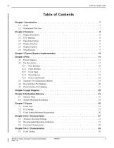
Table of Contents Chapter 1 Introduction . . . . . . . . . . . . . . . . . . . . . . . . . . . . . . . . . . . . 7 1.1 Scope . . . . . . . . . . . . . . . . . . . . . . . . . . . . . . . . . . . 7 1.2 Operational Overview . . . . . . . . . . . . . . . . . . . . . . . . . . . . 7 Chapter 2 Features . . . . 2.1 Display Resolution 2.2 CPU Interface . . 2.3 Input Data Format . 2.4 Display Interface . 2.5 Display Features . 2.6 Miscellaneous . . Chapter 3 Typical System Implementation . . . . . . . . . . . . . . . . . . . . . . . . 10 Chapter 4 Pins . . . . . . . . . . . . . 4.1 Pinout Diagram . ....
Open the catalog to page 3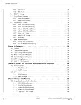
Chapter 11 Indirect and Serial Host Interface Accessing Sequence . . . . 11.1 Indirect Interface . . . . . . . . . . . . . . . . . . . . . . . . 11.1.1 Write Procedure . . . . . . . . . . . . . . . . . . . . . . . . . . . . . 11.1.2 Read Procedure . . . . . . . . . . . . . . . . . . . . . . . . . . . . . 11.2 SPI . . . . . . . . . . . . . . . . . . . . . . . . . . . . . 11.2.1 Write Procedure . . . . . . . . . . . . . . . . . . . . . . . . . . . . . 11.2.2 Read Procedure . . . . . . . . . . . . . . . . . . . . . . . . . . . . . Chapter 12 Image Data Formats . . . . . . 12.1 Image Data Formats...
Open the catalog to page 4
12.2 Data Expansion . . . . . . . . . . . . . . . . . . . . . . . . . . . . . . 100 12.3 Color Depth . . . . . . . . . . . . . . . . . . . . . . . . . . . . . . . 100 Chapter 13 Look-Up Table Architecture 13.1 24 bpp LUT . . . . . . . . . . 13.2 16 bpp LUT . . . . . . . . . . 13.3 8 bpp LUT in Color Mode . . . . Chapter 14 Display Features . . . . . . 14.1 PIP (Picture-in-Picture) Layer . . 14.2 Transparency . . . . . . . . . 14.3 Alpha Blending . . . . . . . . 14.4 PIP Effects . . . . . . . . . . 14.4.1 Blinking and Fading Effects . 14.4.2 Blink/Fade Period . . . . . . 14.4.3 Fade Steps . ....
Open the catalog to page 5
S1D13L01 Series Hardware Functional Specification (Rev. 1.0)
Open the catalog to page 6
Chapter 1 Introduction 1.1 Scope This is the Hardware Functional Specification for the S1D13L01 Series Simple LCD Controller. Included in this document are timing diagrams, AC and DC characteristics, register descriptions, and power management descriptions. This document is intended for two audiences: Video Subsystem Designers and Software Developers. This document is updated as appropriate. Please check for the latest revision of this document before beginning any development. The latest revision can be downloaded at vdc.epson.com. We appreciate your comments on our documentation. Please contact...
Open the catalog to page 7
Chapter 2 Features 2.1 Display Resolution • 384K bytes of embedded VRAM for storing the image data • Display Resolutions for one layer display (Main Layer Only): • Up to 480x272 at 24 bpp • Up to 800x480 at 8 bpp • Display Resolutions for two layer display (Main and PIP Layer): • Up to 400x240 at 24 bpp (Main Layer) and 400x240 at 8 bpp (PIP Layer) 2.2 CPU Interface • 8/16-bit Direct interface • 8/16-bit Indirect interface • SPI (Mode 0, Mode 3) 2.3 Input Data Format • RGB 8:8:8, RGB 5:6:5, 8 bpp grayscale, or 8/16/24 bpp with Look-Up Table (LUT) 2.4 Display Interface • Active Matrix TFT panels...
Open the catalog to page 8
2.5 Display Features • Up to two display layers: • Main Layer • 8/16/24 bpp color depths with optional Look-up Table (LUT) • Independent rotation (0, 90, 180, 270° counter-clockwise) • PIP Layer • 8/16/24 bpp color depths with optional Look-up Table (LUT) • Independent rotation (0, 90, 180, 270° counter-clockwise) • Configurable PIP Effects allow automatic blink and fade in/out effects • Alpha Blending • Transparency • Look-up Tables for Main and PIP Layers (256 address x 24 bpp) 2.6 Miscellaneous • Single Clock Input: CLKI • Embedded PLL • Software initiated Power Save Modes • General Purpose...
Open the catalog to page 9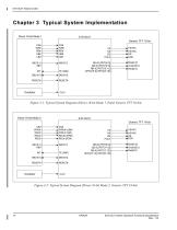
Chapter 3 Typical System Implementation Direct 16-bit Mode 1 Figure 3-1: Typical System Diagram (Direct 16-bit Mode 1, Panel Generic TFT 16-bit) Figure 3-2: Typical System Diagram (Direct 16-bit Mode 2, Generic TFT 18-bit) S1D13L01 Series Hardware Functional Specification (Rev. 1.0)
Open the catalog to page 10
Figure 3-3: Typical System Diagram (Indirect 16-bit Mode 1, Generic TFT 16-bit) Figure 3-4: Typical System Diagram (Indirect 16-bit Mode 2, Generic TFT 18-bit) S1D13L01 Series Hardware Functional Specification (Rev. 1.0)
Open the catalog to page 11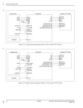
Figure 3-5: Typical System Diagram (Direct 8-bit, Generic TFT 16-bit) Figure 3-6: Typical System Diagram (Indirect 8-bit, Generic TFT 18-bit) S1D13L01 Series Hardware Functional Specification (Rev. 1.0)
Open the catalog to page 12
Figure 3-7: Typical System Diagram (SPI, Generic TFT 24-bit) S1D13L01 Series Hardware Functional Specification (Rev. 1.0)
Open the catalog to page 13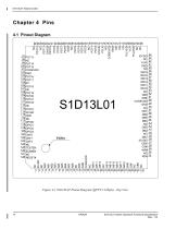
Chapter 4 Pins 4.1 Pinout Diagram IOVDD NC CLKI GND NC DB15 DB14 DB13 DB12 DB11 DB10 NC DB9 DB8 COREVDD GND NC DB7 DB6 DB5 DB4 NC DB3 DB2 NC DB1 IOVDD DB0 CS# WR# NC RD# PDT9 PDT8 PDT7 PDT6 GND NC PDT5 PDT4 PDT3 PDT2 NC PDT1 PDT0 IOVDD PCLK NC COREVDD GND DE HS VS PLLVDD VCP PLLGND NC NC Figure 4-1 S1D13L01 Pinout Diagram (QFP15-128pin) - Top View S1D13L01 Series Hardware Functional Specification (Rev. 1.0)
Open the catalog to page 14
Input Output Bi-Directional (Input/Output) Power pin Analog Power pin Ground Analog Ground RESET# / Power Save State H = High level output L = Low level output Hi-Z = High Impedance Q = Output Pin, retains output state QB = IO Pin, if configured as output retains state Table 4-1: Cell Description Item H System LVCMOS Schmitt Input Buffer with Fail Safe H System LVCMOS Schmitt Input Buffer with pull-down resistor and Fail Safe H System LVCMOS Schmitt Input Buffer with pull-up resistor and Fail Safe H System LVCMOS Input Buffer with pull-down resistor and Fail Safe H System LVCOMOS Output buffer...
Open the catalog to page 15All TOPWAY LCD catalogs and technical brochures
 TOPWAY Smart LCD SGTools Handbook
108 Pages
 10.1" TFT LCD Module
1 Page
 MONO Product
2 Pages
 LMT050DNCFWU-NNA-2
15 Pages
 LMT080TDGP01
16 Pages
 HKT035BTB-1D
36 Pages
 HMT050AMC-C
17 Pages
 HMT043ATA-6C
31 Pages
 TM035PDHG09
42 Pages
 TM035PDHG03
31 Pages
 TM028HDZP01
28 Pages
 LM256160DCW-1
14 Pages
 LM12896FCW-1
17 Pages
 LM12832KCW
13 Pages
 LM2088EFW-9
12 Pages
 LM3122AGG-2
12 Pages
 LM240160YCW
18 Pages
 LM6093ACW
14 Pages
 HMT104ATA-C
11 Pages
 HMT101ATA-D
36 Pages
 HKT080ATA-C
1 Page
 HMT080ATA
1 Page
 HKT070DTA-1C
11 Pages
 HMT070DTA-D
1 Page
 HKT070DMC-2C
19 Pages
 HMT070ETD-C
31 Pages
 HMT070ETD-1D
34 Pages
 HMT056ATA-C
1 Page
 HMT050CB-1C
31 Pages
 HMT050DTA-D
1 Page
 HKT050ATA-C
1 Page
 HMT043ATA-7C
32 Pages
 HMT043GTA-1D
37 Pages
 HKT043BMC-2C
17 Pages
 HMT043ATA-3C
11 Pages
 HMT043BMC-C
1 Page
 HMT043ATA-4C
11 Pages
 HKT043BMC-C
1 Page
 HKT043ATA-1C
12 Pages
 HMT035ATA-D
13 Pages
 HMT028ATB-C
12 Pages
 HKT104ATA-C
31 Pages
 HMT068BTA-C
33 Pages
 HMT070ATA-1C
32 Pages
 HMT080ATA-C
33 Pages
 HMT090ATA-C
30 Pages
 HMT101ATA-C
33 Pages
 HMT050ATA-2C
31 Pages
 HMT043ATA-2C
32 Pages
 IC Raio RA6963 LCD Controller
42 Pages
 IC EPSON S1D13700 LCD Controller
133 Pages
 EPSON S1D13709 LCD Controller
192 Pages
 Samsung S6B0108 LCD Driver
23 Pages
 Avant SBN0064G LCD Driver
37 Pages
 Avant SBN6400G LCD Driver
34 Pages
 EPSON SED1335 LCD Controller
95 Pages
 SGS-THOMSON ST7282
23 Pages
 Raio RA6963 LCD Controller
42 Pages
 Raio RA8875 TFT LCD Controller
174 Pages
 Raio RA8835 LCD Controller
93 Pages
 RAIO RA8803 LCD Controller
8 Pages
 HMT035ATA-1C
1 Page
 Smart LCD introduction
14 Pages
 Topway company introduction
14 Pages
 TFT module in bezel
1 Page
 Topway TFT LCD
1 Page
 LM12864L Series
1 Page
 LM12864T Series
1 Page
 LM12864F Series
1 Page
 LM6060C Series
1 Page
 LM12864M Series
1 Page
 LM6029A Series
1 Page
 LM6059B Series
1 Page
 LM24048A Series
1 Page
 LM13232A Series
1 Page
 LM160160A Series
1 Page
 LMB402C Series
1 Page
 LMB242A Series
1 Page
 LMB204C Series
1 Page
 LM3121 Series
1 Page
 LMB404A Series
1 Page
 HMT043FC-1C
1 Page
 LM3123 Series
1 Page
 LMB204B Series
1 Page
 LMB202E Series
1 Page
 LMB202D Series
1 Page
 LMB164A Series
1 Page
 LMB162G Series
1 Page
 LMB162H Series
1 Page
 LMB162N Series
1 Page
 LMB162A Series
1 Page
 LMB0820D Series
1 Page
 LMB0820C Series
1 Page
 LMB0820A Series
1 Page
 LMB081N Series
1 Page
 LMB081A Series
1 Page
 LMB162X series
1 Page
 LMT057DNAFWU-AAN series
1 Page
 LMT057DNAFWU-AAA series
1 Page
 LMT104SDH01 Series
1 Page
 TOPWAY Product List (Y2012)
4 Pages
 TFT LCD module
1 Page
 Without controller
1 Page
 Chinese fonts
1 Page
 Built-in controller
1 Page
 Character module
1 Page


- Bourn And Koch touch screen monitor
- Bourn And Koch industrial monitor
- Bourn And Koch LCD display
- Bourn And Koch HDMI monitor
- Bourn And Koch VESA mounting monitor
- Bourn And Koch industrial display
- Bourn And Koch TFT LCD display
- Bourn And Koch IP65 monitor
- Bourn And Koch touch screen display
- Bourn And Koch color display
- LED display panel
- Bourn And Koch high-brightness monitor
- Bourn And Koch TFT monitor
- Bourn And Koch electronic display
- Control display system
- Bourn And Koch wall-mount monitor
- IPS display panel
- Bourn And Koch backlit display
- Programmable display system