- Catalogs
- TOPWAY LCD
- EPSON SED1335 LCD Controller
- Company
- Products
- Catalogs
- News & Trends
- Exhibitions
EPSON SED1335 LCD Controller
1 /95Pages

EPSON SED1335 LCD Controller
1 /95Pages
Catalog excerpts
No part of this material may be reproduced or duplicated in any form or by any means without the written permission of Seiko Epson. Seiko Epson reserves the right to make changes to this material without notice. Seiko Epson does not assume any liability of any kind arising out of any inaccuracies contained in this material or due to its application or use in any product or circuit and, further, there is no representation that this material is applicable to products requiring high level reliability, such as, medical products. Moreover, no license to any intellectual property rights is granted...
Open the catalog to page 2
SED1335 Series Technical Manual
Open the catalog to page 3
SED1335 Series Technical Manual
Open the catalog to page 4
SED1335 Series Technical Manual
Open the catalog to page 5
The SED1335 series is a controller IC that can display text and graphics on LCD panel. The SED1335 series can display layered text and graphics, scroll the display in any direction and partition the display into multiple screens. The SED1335 series stores text, character codes and bitmapped graphics data in external frame buffer memory. Display controller functions include transferring data from the controlling microprocessor to the buffer memory, reading memory data, converting data to display pixels and generating timing signals for the buffer memory, LCD panel. The SED1335 series has an internal...
Open the catalog to page 6
BLOCK DIAGRAM Input/Output Register Display Address Controller Refresh Counter Layered Controller Microprocessor Interface Cursor Address Controller SED1335 Series Technical Manual
Open the catalog to page 7
VD4 VD5 VD6 VD7 YSCL YD YDIS WF LP VSS XSCL XECL XD0 XD1 XD2 SED1335 Series Technical Manual
Open the catalog to page 8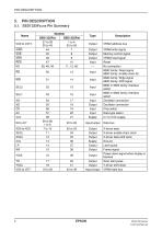
Output Output Output Input — VRAM write signal Memory control signal VRAM read signal Reset No connection 8080 family: Read signal 6800 family: Enable clock (E) 8080 family: Write signal 6800 family: R/W signal 8080 or 6800 family interface select 8080 or 6800 family interface select Oscillator connection Oscillator connection Chip select Data type select 2.7 to 5.5V supply Input Output Input Input Supply Output Output Output Supply Output Output Output Output Input/output D0 to D7 XD0 to XD3 XECL XSCL VSS LP WF YDIS YD YSCL VD0 to VD7 Data bus X-driver data X-driver enable chain clock X-driver...
Open the catalog to page 9
5.2. Pin Functions 5.2.1. Power supply Pin Name VDD VSS Function 2.7 to 5.5V supply. This may be the same supply as the controlling microprocessor. Ground Note: The peak supply current drawn by the SED1335 series may be up to ten times the average supply current. The power supply impedance must be kept as low as possible by ensuring that supply lines are sufficiently wide and by placing 0.47 µF decoupling capacitors that have good high-frequency response near the device’s supply pins. Function Crystal connection for internal oscillator (See section 13). This pin can be driven by an external clock...
Open the catalog to page 10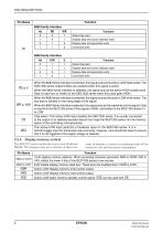
Function 8080 family interface A0 Status flag read Display data and cursor address read Display data and parameter write Command write Status flag read Display data and cursor address read Display data and parameter write Command write When the 8080 family interface is selected, this signal acts as the active-LOW read strobe. The SED1335 series output buffers are enabled when this signal is active. When the 6800 family interface is selected, this signal acts as the active-HIGH enable clock. Data is read from or written to the SED1335 series when this clock goes HIGH. When the 8080 family interface...
Open the catalog to page 11
5.2.5. LCD drive signals In order to provide effective low-power drive for LCD matrixes, the SED1335 series can directly control both the X- and Y-drivers using an enable chain. Pin Name 4-bit X-driver (column drive) data outputs. Connect these outputs to the inputs of the X-driver chips. XSCL=clock XECL LP=latch The falling edge of XSCL latches the data on XD0 to XD3 into the input shift registers of the X-drivers. To conserve power, this clock halts between LP and the start of the following display line (See section 6.3.7). The falling edge of XECL triggers the enable chain cascade for the...
Open the catalog to page 12
Supply voltage Register data retention voltage Input leakage current Output leakage current Operating supply current Quiescent supply current Oscillator frequency External clock frequency Oscillator feedback resistance TTL HIGH-level input voltage LOW-level input voltage Measured at crystal, 47.5% duty cycle. See note 6. HIGH-level output voltage LOW-level output voltage CMOS HIGH-level input voltage LOW-level input voltage HIGH-level output voltage VIHC VILC VOHC LOW-level output voltage Open-drain LOW-level output voltage Schmitt-trigger Rising-edge threshold voltage Falling-edge threshold...
Open the catalog to page 13
VDD = 2.7 to 4.5 V, VSS = 0 V, Ta = –20 to 75˚C unless otherwise noted Rating Parameter Supply voltage Register data retention voltage Input leakage current Output leakage current Operating supply current Quiescent supply current Oscillator frequency External clock frequency Oscillator feedback resistance HIGH-level input voltage LOW-level input voltage HIGH-level output voltage LOW-level output voltage HIGH-level input voltage LOW-level input voltage HIGH-level output voltage LOW-level output voltage Open-drain LOW-level output voltage Schmitt-trigger Rising-edge threshold voltage Falling-edge...
Open the catalog to page 14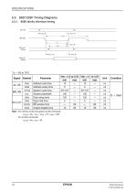
6.3. SED1335F Timing Diagrams 6.3.1. 8080 family interface timing AO, CS tAW8 Parameter Address hold time Address setup time System cycle time Strobe pulsewidth Data setup time Data hold time RD access time Output disable time Note: For memory control and system control commands: tCYC8 = 2tC + tCC + tCEA + 75 > tACV + 245 For all other commands: tCYC8 = 4tC + tCC + 30
Open the catalog to page 15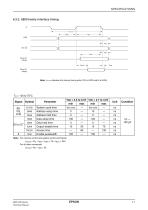
6.3.2. 6800 family interface timing E tCYC6 tAW6 Note: tCYC6 indicates the interval during which CS is LOW and E is HIGH. System cycle time Address setup time Address hold time Data setup time Data hold time Output disable time Access time Enable pulsewidth Note: For memory control and system control commands: tCYC6 = 2tC + tEW + tCEA + 75 > tACV + 245 For all other commands: tCYC6 = 4tC + tEW + 30
Open the catalog to page 16All TOPWAY LCD catalogs and technical brochures
 TOPWAY Smart LCD SGTools Handbook
108 Pages
 10.1" TFT LCD Module
1 Page
 MONO Product
2 Pages
 LMT050DNCFWU-NNA-2
15 Pages
 LMT080TDGP01
16 Pages
 HKT035BTB-1D
36 Pages
 HMT050AMC-C
17 Pages
 HMT043ATA-6C
31 Pages
 TM035PDHG09
42 Pages
 TM035PDHG03
31 Pages
 TM028HDZP01
28 Pages
 LM256160DCW-1
14 Pages
 LM12896FCW-1
17 Pages
 LM12832KCW
13 Pages
 LM2088EFW-9
12 Pages
 LM3122AGG-2
12 Pages
 LM240160YCW
18 Pages
 LM6093ACW
14 Pages
 HMT104ATA-C
11 Pages
 HMT101ATA-D
36 Pages
 HKT080ATA-C
1 Page
 HMT080ATA
1 Page
 HKT070DTA-1C
11 Pages
 HMT070DTA-D
1 Page
 HKT070DMC-2C
19 Pages
 HMT070ETD-C
31 Pages
 HMT070ETD-1D
34 Pages
 HMT056ATA-C
1 Page
 HMT050CB-1C
31 Pages
 HMT050DTA-D
1 Page
 HKT050ATA-C
1 Page
 HMT043ATA-7C
32 Pages
 HMT043GTA-1D
37 Pages
 HKT043BMC-2C
17 Pages
 HMT043ATA-3C
11 Pages
 HMT043BMC-C
1 Page
 HMT043ATA-4C
11 Pages
 HKT043BMC-C
1 Page
 HKT043ATA-1C
12 Pages
 HMT035ATA-D
13 Pages
 HMT028ATB-C
12 Pages
 HKT104ATA-C
31 Pages
 HMT068BTA-C
33 Pages
 HMT070ATA-1C
32 Pages
 HMT080ATA-C
33 Pages
 HMT090ATA-C
30 Pages
 HMT101ATA-C
33 Pages
 HMT050ATA-2C
31 Pages
 HMT043ATA-2C
32 Pages
 IC Raio RA6963 LCD Controller
42 Pages
 IC Epson S1D13L01 LCD Controller
118 Pages
 IC EPSON S1D13700 LCD Controller
133 Pages
 EPSON S1D13709 LCD Controller
192 Pages
 Samsung S6B0108 LCD Driver
23 Pages
 Avant SBN0064G LCD Driver
37 Pages
 Avant SBN6400G LCD Driver
34 Pages
 SGS-THOMSON ST7282
23 Pages
 Raio RA6963 LCD Controller
42 Pages
 Raio RA8875 TFT LCD Controller
174 Pages
 Raio RA8835 LCD Controller
93 Pages
 RAIO RA8803 LCD Controller
8 Pages
 HMT035ATA-1C
1 Page
 Smart LCD introduction
14 Pages
 Topway company introduction
14 Pages
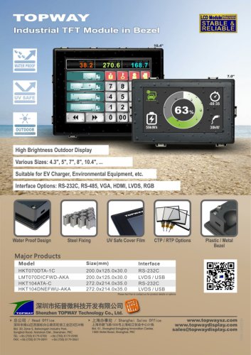 TFT module in bezel
1 Page
 Topway TFT LCD
1 Page
 LM12864L Series
1 Page
 LM12864T Series
1 Page
 LM12864F Series
1 Page
 LM6060C Series
1 Page
 LM12864M Series
1 Page
 LM6029A Series
1 Page
 LM6059B Series
1 Page
 LM24048A Series
1 Page
 LM13232A Series
1 Page
 LM160160A Series
1 Page
 LMB402C Series
1 Page
 LMB242A Series
1 Page
 LMB204C Series
1 Page
 LM3121 Series
1 Page
 LMB404A Series
1 Page
 HMT043FC-1C
1 Page
 LM3123 Series
1 Page
 LMB204B Series
1 Page
 LMB202E Series
1 Page
 LMB202D Series
1 Page
 LMB164A Series
1 Page
 LMB162G Series
1 Page
 LMB162H Series
1 Page
 LMB162N Series
1 Page
 LMB162A Series
1 Page
 LMB0820D Series
1 Page
 LMB0820C Series
1 Page
 LMB0820A Series
1 Page
 LMB081N Series
1 Page
 LMB081A Series
1 Page
 LMB162X series
1 Page
 LMT057DNAFWU-AAN series
1 Page
 LMT057DNAFWU-AAA series
1 Page
 LMT104SDH01 Series
1 Page
 TOPWAY Product List (Y2012)
4 Pages
 TFT LCD module
1 Page
 Without controller
1 Page
 Chinese fonts
1 Page
 Built-in controller
1 Page
 Character module
1 Page


- Monitor with touchscreen
- Industrial monitor
- LCD display panel
- HDMI monitor
- VESA mounting monitor
- Industrial display panel
- TFT display module
- IP65 monitor
- Touch screen display panel
- Color display panel
- LED display panel
- High-brightness monitor
- TFT-LCD monitor
- Electronic display panel
- Control display system
- Wall-mount monitor
- IPS display panel
- Backlit display panel
- Programmable display system