
- Catalogs
- TOPWAY LCD
- Avant SBN0064G LCD Driver


- Company
- Products
- Catalogs
- News & Trends
- Exhibitions
Avant SBN0064G LCD Driver

Avant SBN0064G LCD Driver
Catalog excerpts
DATA SHEET SBN0064G Dot-matrix STN LCD 64-SEGMENT Driver with 64-row x 64-column Display Data Memory To improve design and/or performance, Avant Electronics may make changes to its products. Please contact Avant Electronics for the latest versions of its products
Open the catalog to page 1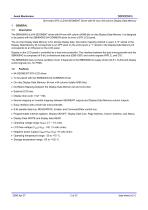
Avant Electronics Dot-matrix STN LCD 64-SEGMENT Driver with 64-row x 64-column Display Data Memory 1 The SBN0064G is a 64-SEGMENT driver with 64-row x64 column (4096-bit) on-chip Display Data Memory. It is designed to be paired with the SBN6400G 64-COMMON driver to drive a STN LCD panel. The on-chip Display Data Memory is for storing display data. Dot-matrix mapping method is used. A “0” stored in the Display Data Memory bit corresponds to an OFF-pixel on the LCD panel; a “1” stored in the Display Data Memory bit corresponds to an ON-pixel on the LCD panel. Display on the LCD panel is controlled...
Open the catalog to page 2
Avant Electronics Dot-matrix STN LCD 64-SEGMENT Driver with 64-row x 64-column Display Data Memory 1.3 Ordering information Ordering information PRODUCT TYPE
Open the catalog to page 3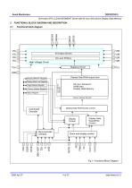
Avant Electronics Dot-matrix STN LCD 64-SEGMENT Driver with 64-row x 64-column Display Data Memory FUNCTIONAL BLOCK DIAGRAM AND DESCRIPTION Functional block diagram High Voltage Circuit Mapping Circuit CSM Display Data RAM output latch Display ON/OFF Register Display Start Line Register 64 row x 64column (4096 bits) Display Data Memory Line Address Decoder Page Address Register Column Address Register Status Register Column Address Decoder Display Data RAM Access Control Display Data Read/Write Control Display Control Clock and display control Microcontroller Interface Command Decoder Fig.1 Functional...
Open the catalog to page 4
Avant Electronics Dot-matrix STN LCD 64-SEGMENT Driver with 64-row x 64-column Display Data Memory 3 PIN(PAD) ASSIGNMENT, PAD COORDINATES, SIGNAL DESCRIPTION The SBN0064G pinning diagram (LQFP100)
Open the catalog to page 5
Avant Electronics Dot-matrix STN LCD 64-SEGMENT Driver with 64-row x 64-column Display Data Memory The total pad number is 97. The chip ID is located at the lower left part of the chip. The chip ID of is 18005. The die origin is at the center of the chip. (5) For chip_on_board bonding, chip carrier should be connected to VDD or left open. Chip carrier is the metal pad to which the die is attached.
Open the catalog to page 6
Avant Electronics Dot-matrix STN LCD 64-SEGMENT Driver with 64-row x 64-column Display Data Memory 3.3
Open the catalog to page 7
Avant Electronics Dot-matrix STN LCD 64-SEGMENT Driver with 64-row x 64-column Display Data Memory 3.4 Signal description Table 3 Pad signal description To avoid a latch-up effect at power-on: VSS − 0.5 V < voltage at any pin at any time < VDD + 0.5 V . Pad number DESCRIPTION Column/Segment Mapping. This signal controls the mapping relation between the column output of the Display Data Memory and the SBN0064G’s segment output. If CMS=1, the mapping is called Normal Mapping. The mapping relation is that Columns 0, 1, 2,...,62,63 of the Display Data Memory are mapped to Segments 0, 1, 2,..., 62,...
Open the catalog to page 8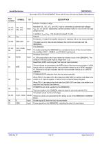
Avant Electronics Dot-matrix STN LCD 64-SEGMENT Driver with 64-row x 64-column Display Data Memory Pad number DESCRIPTION External LCD Bias voltage. Note that V0L, V2L, V3L, and V5L must be connected to external bias voltages VDD, V2, V3, and V5, respectively, and the condition VDD≥V1≥V2≥V3≥V4≥V5 must always be met. In addition, VLCD (VDD - V5) should not exceed 13 volts. Ground. Bi-direction, tri-state 8-bit parallel data bus for interface with a host microcontroller. This data bus is for data transfer between the host microcontroller and the SBN0064G. Chip Selection To enable selecting the...
Open the catalog to page 9
Avant Electronics Dot-matrix STN LCD 64-SEGMENT Driver with 64-row x 64-column Display Data Memory 4 A SBN6400G and SBN0064G-based display system is shown in Fig. 5. The SBN6400G contains timing generation circuit and 64 COMMON drivers. The timing generation circuit generates operating clocks and display control signals (frame signal FRM , COMMON scan signal CL, and AC frame signal M), for itself and the SBN0064G. The SBN0064G contains 64 SEGMENT drivers, Display Data Memory, and interface circuit with a host microcontroller. Data bus Microcontroller Interface Display Data Memory Host microcontroller...
Open the catalog to page 10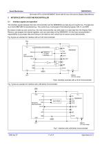
Avant Electronics Dot-matrix STN LCD 64-SEGMENT Driver with 64-row x 64-column Display Data Memory 5 INTERFACE WITH A HOST MICROCONTROLLER Interface signals and operation The interface signals between the host microcontroller and the SBN0064G are data bus and control bus. The data bus is an 8-bit (DB0~DB7) bi-directional bus. The control bus is composed of the following signals: C/D, E, and R/W. By means of data bus and control bus, the host microcontroller can write data to or read data from the Display Data Memory, can program the internal registers, and can read status of the SBN0064G. It...
Open the catalog to page 11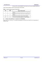
Avant Electronics Dot-matrix STN LCD 64-SEGMENT Driver with 64-row x 64-column Display Data Memory Table 4 lists the setting for control bus and the types of data transfer. Table 4 Interface signals and types of data transfer Types of data transfer The host microcontroller reads data from the Display Data Memory. The host microcontroller writes data to the Display Data Memory The host microcontroller reads the Status Register. The host microcontroller programs an internal register. Interface Timing (Writing to or reading from the SBN0064G) Please refer to Fig. 16 and Fig. 17 for interface timing...
Open the catalog to page 12
Avant Electronics Dot-matrix STN LCD 64-SEGMENT Driver with 64-row x 64-column Display Data Memory 6 DISPLAY DATA MEMORY AND LCD DISPLAY The Display Data Memory is a static memory bit(cell) array of 64-row x 64-column. So, the total bit number is 64 x 64 = 4096 bits (512 bytes). Each bit of the memory is mapped to a single pixel (dot) on the LCD panel. A “1” stored in the Display Data Memory bit corresponds to an ON pixel (black dot in normal display). A “0” stored in the Display Data Memory bit corresponds to an OFF pixel (background dot in normal display). Column outputs (Column 0~63) of the...
Open the catalog to page 13All TOPWAY LCD catalogs and technical brochures
 TOPWAY Smart LCD SGTools Handbook
108 Pages
 10.1" TFT LCD Module
1 Page
 MONO Product
2 Pages
 LMT050DNCFWU-NNA-2
15 Pages
 LMT080TDGP01
16 Pages
 HKT035BTB-1D
36 Pages
 HMT050AMC-C
17 Pages
 HMT043ATA-6C
31 Pages
 TM035PDHG09
42 Pages
 TM035PDHG03
31 Pages
 TM028HDZP01
28 Pages
 LM256160DCW-1
14 Pages
 LM12896FCW-1
17 Pages
 LM12832KCW
13 Pages
 LM2088EFW-9
12 Pages
 LM3122AGG-2
12 Pages
 LM240160YCW
18 Pages
 LM6093ACW
14 Pages
 HMT104ATA-C
11 Pages
 HMT101ATA-D
36 Pages
 HKT080ATA-C
1 Page
 HMT080ATA
1 Page
 HKT070DTA-1C
11 Pages
 HMT070DTA-D
1 Page
 HKT070DMC-2C
19 Pages
 HMT070ETD-C
31 Pages
 HMT070ETD-1D
34 Pages
 HMT056ATA-C
1 Page
 HMT050CB-1C
31 Pages
 HMT050DTA-D
1 Page
 HKT050ATA-C
1 Page
 HMT043ATA-7C
32 Pages
 HMT043GTA-1D
37 Pages
 HKT043BMC-2C
17 Pages
 HMT043ATA-3C
11 Pages
 HMT043BMC-C
1 Page
 HMT043ATA-4C
11 Pages
 HKT043BMC-C
1 Page
 HKT043ATA-1C
12 Pages
 HMT035ATA-D
13 Pages
 HMT028ATB-C
12 Pages
 HKT104ATA-C
31 Pages
 HMT068BTA-C
33 Pages
 HMT070ATA-1C
32 Pages
 HMT080ATA-C
33 Pages
 HMT090ATA-C
30 Pages
 HMT101ATA-C
33 Pages
 HMT050ATA-2C
31 Pages
 HMT043ATA-2C
32 Pages
 IC Raio RA6963 LCD Controller
42 Pages
 IC Epson S1D13L01 LCD Controller
118 Pages
 IC EPSON S1D13700 LCD Controller
133 Pages
 EPSON S1D13709 LCD Controller
192 Pages
 Samsung S6B0108 LCD Driver
23 Pages
 Avant SBN6400G LCD Driver
34 Pages
 EPSON SED1335 LCD Controller
95 Pages
 SGS-THOMSON ST7282
23 Pages
 Raio RA6963 LCD Controller
42 Pages
 Raio RA8875 TFT LCD Controller
174 Pages
 Raio RA8835 LCD Controller
93 Pages
 RAIO RA8803 LCD Controller
8 Pages
 HMT035ATA-1C
1 Page
 Smart LCD introduction
14 Pages
 Topway company introduction
14 Pages
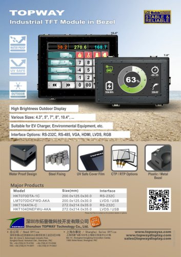 TFT module in bezel
1 Page
 Topway TFT LCD
1 Page
 LM12864L Series
1 Page
 LM12864T Series
1 Page
 LM12864F Series
1 Page
 LM6060C Series
1 Page
 LM12864M Series
1 Page
 LM6029A Series
1 Page
 LM6059B Series
1 Page
 LM24048A Series
1 Page
 LM13232A Series
1 Page
 LM160160A Series
1 Page
 LMB402C Series
1 Page
 LMB242A Series
1 Page
 LMB204C Series
1 Page
 LM3121 Series
1 Page
 LMB404A Series
1 Page
 HMT043FC-1C
1 Page
 LM3123 Series
1 Page
 LMB204B Series
1 Page
 LMB202E Series
1 Page
 LMB202D Series
1 Page
 LMB164A Series
1 Page
 LMB162G Series
1 Page
 LMB162H Series
1 Page
 LMB162N Series
1 Page
 LMB162A Series
1 Page
 LMB0820D Series
1 Page
 LMB0820C Series
1 Page
 LMB0820A Series
1 Page
 LMB081N Series
1 Page
 LMB081A Series
1 Page
 LMB162X series
1 Page
 LMT057DNAFWU-AAN series
1 Page
 LMT057DNAFWU-AAA series
1 Page
 LMT104SDH01 Series
1 Page
 TOPWAY Product List (Y2012)
4 Pages
 TFT LCD module
1 Page
 Without controller
1 Page
 Chinese fonts
1 Page
 Built-in controller
1 Page
 Character module
1 Page



- Touch monitor
- LCD screen
- Industrial monitor
- HDMI monitor
- Industrial display panel
- VESA mounting monitor
- TFT display module
- Color display panel
- Touch screen display panel
- LED display panel
- High-brightness monitor
- IPS display panel
- TFT-LCD monitor
- Control display system
- Electronic display panel
- Backlit display panel
- Wall-mount monitor
- LED-backlit display panel