- Catalogs
- Tokyo Diamond Tools Mfg. Co., Ltd.
- Vitrified bond diamond grinding wheel for compound semiconductor wafer (Fine)
Vitrified bond diamond grinding wheel for compound semiconductor wafer (Fine)
1 /1Page

Vitrified bond diamond grinding wheel for compound semiconductor wafer (Fine)
1 /1Page
Catalog excerpts
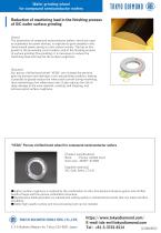
Wafer grinding wheel for compound semiconductor wafers Reduction of machining load in the finishing process of SiC wafer surface grinding [Issue] The production of compound semiconductor wafers, which are used as substrates for power devices, is expected to grow steadily in the trend toward power saving in a low-carbon society. The key to this growth is the processing cost of wafers, and in the finishing process of surface grinding (fine grinding), it is necessary to reduce the machining load and improve the surface roughness. [Solution] Our porous vitrified bond wheel "VEGA" can increase the abrasive grain tip pressure and maintain a non-slip grinding condition, making it possible to greatly reduce the wheel axial current during machining, thus maintaining a low wheel wear rate. It also reduces the risk of deep damage to the work material, cracking, and chipping, and achieves good surface roughness. “VEGA” Porous vitrified bond wheel for compound semiconductor wafers [Product specifications] Bond : Porous vitrified bond Grain size : #4000~#12000 [Applied materials] SiC, GaN, GaAs, LT/LN ■Higher surface roughness is realized by the combination of ultra-fine diamond abrasive grains and vitrified bonds of large and fine porous combination structure. ■Spontaneous blade generation is realized and cutting quality is maintained by bonds that can make ultrafine shredding. ■Stable high-quality surface and low processing cost can be realized. 2-3-5 Nakane Meguro-ku Tokyo 152-0031 Japan https://www.tokyodiamond.com/ E-mail: [email protected] Tel : +81-3-3723-8114 [
Open the catalog to page 1All Tokyo Diamond Tools Mfg. Co., Ltd. catalogs and technical brochures
 Tokyo Diamond Catalog
36 Pages


- Milling tool
- Milling tool with replaceable insert
- Metal milling cutter
- End mill
- Cutting milling cutter
- High-performance milling cutter
- Slot milling tool
- Surface treatment wheel
- Diamond milling cutter
- Plastic milling cutter
- High-precision milling cutter
- High-speed milling cutter
- Composite milling cutter
- Cutting tool
- Cylindrical grinding wheel
- Burr
- Surfacing wheel
- Automobile milling cutter
- Diamond grinding wheel
- Chamfer milling cutter