- Catalogs
- Tescan GmbH
- MAIA3
MAIA3
1 /12Pages

MAIA3
1 /12Pages
Catalog excerpts
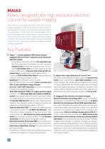
The MAIA3 is an uLtra-high resolution SEM with excellent imaging capabilities in the whole range of beam energies. A versatile detection system and high spatial resolution allows the observation of even the finest surface details. This is an essential feature for comprehensive characterisation of nanomateriaLs, for observation of beam-sensitive samples common in the semiconductor industry and for comfortable imaging of non-conductive samples including uncoated biological specimens. Key Features ■ Triglav™ - a newly designed UHR electron column equipped with the TriLens™ objective and an advanced detection...
Open the catalog to page 2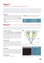
Triglav™ Experience ultimate resolution The new TESCAN SEM column Triglav™ delivers a unique combination of immersion optics and crossover-free mode for UHR imaging at low energies. The single-pole type objective lens creates a magnetic field around the sample and dramatically decreases optical aberrations. Avoiding any crossover in the column reduces the Boersch effect and further optimizes the electron beam to yield superior resolution. Surface details of the specimen can be captured more reliably than ever before. For analysis, the TriLens™ technology improves resolution in the magnetic-field-free...
Open the catalog to page 3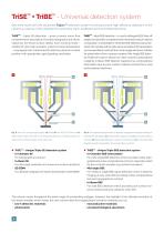
TriSE™ + TriBE™ - Universal detection system See even more with the advanced Triglav™ detection system involving several high-efficiency detectors in the column as well as in the chamber for secondary, back-scattered and transmitted electrons. TriSE™ – triple SE detection – gives a nearly noise-free comprehensive description of sample topography and allows capturing the finest surface details. Each working mode – whether for ultra-high resolution, analysis or beam deceleration – is equipped with a dedicated SE detector placed in an ideal position with appropriate signal guiding electrodes. TriBE™...
Open the catalog to page 4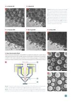
Fig. 5-9: SiN with Ag contact imaged at 5 keV with: (5) The In-Chamber SE detector which delivers excellent topographic contrast and is less sensitive to charging (6) The In-Beam SE detector for ultimate resolution (7) The In-Chamber BSE detector for collecting wide angle BSE giving topographic and material contrast (8) The Mid-Angle BSE detector for material contrast from the whole interaction volume (9) The In-Beam BSE detector for collecting axial BSE for material contrast of uppermost surface layers Beam Deceleration Mode When the beam deceleration mode (BDM) is enabled, the detection system...
Open the catalog to page 5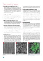
Features highlights High Probe Current and Short Analytical WD The new Schottky FE gun enables beam currents up to 400 nA which are suitable for all analytical techniques such as EDX, WDX, EBSD, CL etc. With the exception of CL, all these detectors are optimised to operate at an analytical working distance of 5 mm, which is short enough to ensure excellent resolution for analysis. In-Flight Beam Tracing™ Very accurate real-time computation of working distance, magnification and all optical parameters together with continuous control of beam spot size and beam current is ensured by In-Flight Beam...
Open the catalog to page 6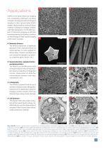
Applications MAIA3 is the ideal choice for imaging non-conductive and beam-sensitive samples including all kinds of biological samples in their natural state. MAIA3 enables highly sensitive surface analysis making it suitable for imaging samples with high topography. It is the SEM system of choice for keeping up with the increasing demand in all fields of science and technology for high-quality imaging at low beam energies. Materials Science The MAIA3 represents a significant advance in the characterisation of nanomaterials. It is also suitable for observation of beam-sensitive and non-conductive...
Open the catalog to page 7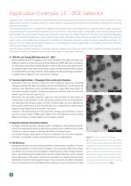
Application Example: LE - BSE detector Imaging of non-conductive samples, detecting nuances of compositional contrast or resolving tiny surface features in many fields of life sciences, materials science or semiconductor engineering have become increasingly important for scanning electron microscopy. With a high energy beam, the penetration depth of the electron beam interacting with the sample surface is high, resulting in a large interaction volume. Modern materials such as very thin - nanometre scale - composites scale cannot be observed at high energies because surface features are transparent...
Open the catalog to page 8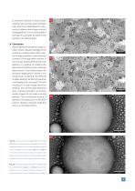
to enhance contrast. In these cases, working at low primary beam energies and using the LE-BSE detector is necessary to obtain clear images without charging effects. Due to lower radiation damage, it is possible to observe the sample in its natural state. Conclusion Reducing the primary beam energy results in lower radiation damage of the specimen, enables observation without charging artifacts, and enhances contrast of the specimen surface. A low energy backscattered electron detector is capable of meeting the demands of modern (nano) materials observations. It is an ideal solution for all those...
Open the catalog to page 9
MAIA3 chamber configurations LM/XM/GM chambers The LM/XM/GM chambers are all equipped with a compucentric fully motorised specimen stage and their optimised geometry allows multiple detectors to be installed. The chambers can be configured to operate either in high vacuum (LMH/XMH/GMH), or variable pressure (LMU/XMU/ GMU) modes - a feature which extends their operations to low vacuum. The LMH/XMH/GMH chambers allow imaging of conductive specimens under high-vacuum conditions while the LMU/XMU/GMU chambers enable imaging of uncoated non-conductive samples under low-vacuum conditions. Extended...
Open the catalog to page 10
■ Electron Optics ■ Detectors* LMH XMH GMH High brightness Schottky emitter Standard mode In-Beam SE 0.7 nm at 15 keV 1.4 nm at 1 keV 1.7 nm at 500 eV Retractable BSE Detector (Motor.) Mid-Angle BSE Detector In-Beam LE-BSE Detector Beam Deceleration Mode (option) STEM detector (optional) 0.7 nm at 30 keV Beam Deceleration Technology (BDT)2 Low Vacuum Secondary Electron TESCAN Detector (LVSTD) STEM Detector Maximum Field of View: Electron beam energy: 200 eV to 30 keV / down to 50 eV with BDT option WiTec Raman (RISE) Multi Image Calibrator 0 Particles Basic □ Particles Advanced □...
Open the catalog to page 11All Tescan GmbH catalogs and technical brochures
 LYRA3
LYRA312 Pages
 VEGA3
VEGA36 Pages
 TESCAN S8000
6 Pages
 TESCAN S9000X
6 Pages
- Microscope
- Laboratory microscope
- Inspection microscope
- Desktop microscope
- Measuring microscope
- Analysis microscope
- Automated microscope
- High-resolution microscope
- Industrial microscope
- Materials research microscope
- Quality control microscope
- Research microscope
- Confocal microscope
- Modular microscope
- Computed tomography machine
- Real-time microscope
- High-precision microscope
- X-ray computed tomography machine
- CT computed tomography machine
- High-contrast microscope