IA-DJ
1 /17Pages

IA-DJ
1 /17Pages
Catalog excerpts

DALSA IA-DJ High Quanta Imaging Sensor Features Front illuminated full-frame CCD High QE response 24 μm × 24 μm pixel size 524×524, 1044×1044, or 2084×2084 pixel resolution Low dark current (< 15 pA/cm2 @ 25 °C) Dark signal noise <1 e- / pixel per second at -16 °C Single output, up to 10 MHz data rate 1×1, 2×2, or 4×4 binning modes High speed Area of Interest (AOI) mode ~100% fill factor (approx.) Photo-sensitive readout registers for real-time exposure monitoring Description The IA-DJ High Quanta full-frame CCD sensors are designed to meet the requirements of scientific and x-ray applications demanding high sensitivity, high frame rates and low noise performance. The High Quanta series of sensors aims to provide the highest quantum efficiency in a front-illuminated sensor. Sensor Block Diagram 4 Dark IA-DJ Imaging Area N (H) x N (V) 24 x 24 μm HCCD - N Active Pixels 4 Dark 4 Inactive
Open the catalog to page 1
DALSA IA-DJ High Quanta Imaging Sensor Gate Structure Diagram The shaded region represents the non-imaging region PIXELS (N x N) Functional Description The IA-DJ sensors are composed of three main functional groups: photo pixels, in which the charge packets are generated, CCD readout shift registers, and output amplifiers where the charge packets are converted to voltage pulses. Detection The IA-DJ sensors are available in 524 × 524, 1044 × 1044, 2084 × 2084 pixel resolutions. The pixels are 24 × 24 μm in size. Light incident on these pixels is converted into charge packets whose size (i.e. the...
Open the catalog to page 2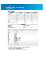
DALSA IA-DJ High Quanta Imaging Sensor Sensor Architecture Image Section Active Image Aspect Ratio Pixel width × height Pixel Optical Fill Factor Number of active lines Number of dark lines Total number of lines No. of active pixels per line No. of dark + inactive pixels per line Total No. of pixels per line Output Amplifier No. Output Amplifier Load Current Sensor Pinout Signal Name CI1 CI2 CILAST VBB VGR VVD VDC CR1 CR2 CRLAST VSET RST VSS VOD VDD OS Output Section 2 stage source follower 1 External Signal Description Vertical CCD Clock - Phase 1 Vertical CCD Clock - Phase 2 Last Vertical CCD...
Open the catalog to page 3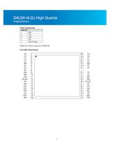
DALSA IA-DJ High Quanta Imaging Sensor Power Sequencing Power On 1 VBB 2 VSS 3 VOD 4 RST 5 Rest of biases POWER OFF: Reverse sequence of POWER ON. IA-DJ-2084 Pinout Drawing
Open the catalog to page 4
Additional Performance Specifications Parameter Full Well Capacity1 (Ne-sat) Charge Conversion Efficiency (CCE) RMS noise2 Dynamic range3 Charge Transfer Efficiency (CTE) Dark current density4 (Jd) Dark current doubling temp Wavelength at peak responsivity Peak responsivity QE OS Linearity5 Anti-blooming Notes: 1. VOD and RST DC biases can be adjusted to increase the Ne-sat. OS linearity may suffer near 200 Ke- Ne-sat. 2. Noise floor of the CCD Amplifier assuming correlated double sampling, data rate = 5 MHz, temperature = 20°C, bandwidth = 17 MHz. 3. 20LOG(Ne-sat/RMS Noise) using typical rms...
Open the catalog to page 5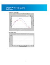
DALSA IA-DJ High Quanta Imaging Sensor Responsivity and QE Graph IA-DJ Spectral Responsivity & Quantum Efficiency Responsivity Q.E. Quantum Efficiency (%) Dark Current Graph IA-DJ Dark Current Density vs Package Temperature Jdark (pA/cm )
Open the catalog to page 6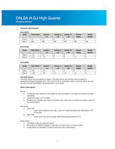
DALSA IA-DJ High Quanta Imaging Sensor Cosmetic Specification IA-DJ-00524 Grade Point Defect Point Defect Test Grade Sensors Test grade sensors may be available, by request. Test grade sensors are functional sensors provided for engineering development purposes only. These sensors have an unspecified number of cosmetic defects and may not meet all sensor specifications. Not all parameters may be tested. Defect Description General: An exclusion zone consisting of the outside two rows and columns on all sides are excluded from defect calculations Specification apply at 25°C ambient Deviations are...
Open the catalog to page 7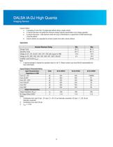
DALSA IA-DJ High Quanta Imaging Sensor Column Defect: • A grouping of more than 10 single pixel defects along a single column • A column that does not exhibit the minimum charge capacity specification (Low charge capacity) • A column that loses >500 electrons when the array is illuminated to a signal level of 2000 electrons/pix. (Trap like defect) • Column defects are separated by at least 5 pixels from other column defects Operation Absolute Maximum Rating Min Max Storage Temp -20 °C 80 °C Operating Temp -20 °C 60 °C Voltage on CI1, CI2, CILAST, VDC, CR1, CR2 with respect to VBB -10 V 18 V Voltage...
Open the catalog to page 8
DALSA IA-DJ High Quanta Imaging Sensor DC Operating Conditions Symbol Description Unit Min. Rec. Max ILOAD Load current to the output (OS) mA 2.0 3.0 5.0 VDD Amplifier Supply V 16.5 17.0 17.5 VOD Output reset drain V 15.0 15.5 16.0 VSET Output node set gate V 1.0 2.0 2.0 VVD AOI Drain V 10.0 12.0 14.0 VSS1 Amplifier Return V 2.0 2.0 2.5 VBB1 Substrate V 0 0 0 VGR Guard Ring V 9.0 10.0 14.0 Note: 1. VBB should never be forward biased with respect to VSS. To protect against damage, a Schottky diode between VBB and VSS is recommended AC Operating Conditions Symbol Description CIx All CIx Clocks...
Open the catalog to page 9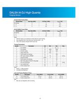
DALSA IA-DJ High Quanta Imaging Sensor IA-DJ-01044 Frame Rate Binning Mode Data Rate (MHz) No binning 5 2×2 5 4×4 5 IA-DJ-02084 Frame Rate Binning Mode Data Rate (MHz) CR Clock1 (MHz) No binning 5 5 2×2 5 10 4×4 5 20* Notes: 1. CRLAST needs to be maintained at Data Rate for proper binning. 2. Zero integration time, max frame rate. Overclock pixel = 20. 3. This is the maximum allowed HCCD clock rate. Timing Parameters Symbol Description t1 CI1 duration t2 CI2 duration t3 CI1/CI2 overlap t4 HCCD setup time t5 HCCD period (no binning) t6 RST pulse duration (FWHM)2 t7 Overclock pixels t8 HCCD period...
Open the catalog to page 10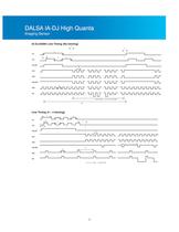
DALSA IA-DJ High Quanta Imaging Sensor IA-DJ-02084 Line Timing (No binning) t4 t7 t1 CI1 Line Timing (4 × 4 binning) t1
Open the catalog to page 11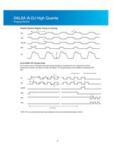
DALSA IA-DJ High Quanta Imaging Sensor Detailed Readout Register Timing (no binning) t10 IA-DJ-02084 AOI Charge Dump IA-DJ sensors have an AOI feature that allows charge dumping of unwanted lines into a charge drain until the desired line is reached. This allows for faster AOI readout. The charge dumping can be initiated by clocking the VDC gate. Last line dump First valid line transfer Line Dump *NOTE: CRs can be clocked during charge dumping to reduce accumulated dark signal on HCCD.
Open the catalog to page 12All Teledyne DALSA catalogs and technical brochures
 Shad-o-Box HS
9 Pages
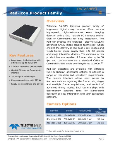 Rad-icon datasheet
7 Pages
 Xcelera-CL+ PX8
2 Pages
 Remote RadEye Family
7 Pages
 Xineos 3131
2 Pages
 Xineos 2121
2 Pages


Archived catalogs
 Sapera APF
4 Pages
 Piranha HS 8k
2 Pages
 1M30
1M302 Pages
 BOA Pro
2 Pages
 Icon
Icon4 Pages
 Piranha3 16k Datasheet
2 Pages
 Pantera 22M04
2 Pages
 Spyder3 Color CL
2 Pages
 FT50M
FT50M2 Pages
 PC2-Comp Express
2 Pages
 Genie HC1024
2 Pages
 Genie C1280
2 Pages
 Falcon2 8M
2 Pages
 Falcon2 4M
2 Pages
 Falcon2 12M
2 Pages
 Falcon 4M60
2 Pages
 Falcon 4M60 Color
2 Pages
 BOA IDR
2 Pages
 Piranha HS 4K 110 kHz
2 Pages
 Xcelera-CL VX4
2 Pages
 Genie M1024
2 Pages
 Genie C1024
2 Pages
 Eclipse
2 Pages
 Falcon 4M30 Color
2 Pages
 Genie HM1400 / HM1400-XDR
2 Pages
 Falcon VGA300 HG
2 Pages
 SkiaGraph Product Family
2 Pages
 BOA
BOA2 Pages
 Spyder3 GigE
2 Pages
 FTF3021M
2 Pages
 IT-P1
IT-P12 Pages
 PC2-Camlink
4 Pages
 X64-AN Quad
4 Pages
 2009 products catalogue
13 Pages
- Liebherr digital camera
- Liebherr visible camera
- CMOS camera module
- Liebherr industrial camera
- Image processing camera module
- Monochrome camera module
- Inspection imager
- High-speed camera module
- Liebherr high-performance camera
- Machine vision video camera
- 3D imager
- Liebherr CMOS image sensor
- X-ray detector
- X-ray flat panel detector
- Flat panel detector
- Liebherr high-resolution image sensor
- Digital flat panel detector
- Time-integration camera