- Catalogs
- Taiwan Semiconductor
- TSH190CT
TSH190CT
1 /8Pages

TSH190CT
1 /8Pages
Catalog excerpts

TSH190Bipolar High Voltage Hall Effect Latch Pin Definition: 1. Vcc 2. GND 3. Output Description TS190, Hall-Effect sensor, designed for electronic commutation of brush-less DC motor applications. The device includes an on-chip Hall voltage generator for magnetic sensing, a comparator that amplifies the Hall Voltage, and a Schmitt trigger to provide switching hysteresis for noise rejection, open collector output. An internal band gap regulator is used to provide temperature compensated supply voltage for internal circuits and allows a wide operating supply range. The device is identical except for magnetic switch points. A south pole of sufficient strength will turn the output on. The North Pole is necessary to turn the output off. An on-board regulator permits operation with supply voltages of 4V to 30 V. Features • Optimized for BLDC motor applications • High Peak Voltage of 65V • 100% tested at 125oC • Temperature compensation function Ordering Information Part No. Note: “G” denote for Halogen Free Product Application • High temperature Fan motor • 3 phase BLDC motor application • Fan motor application • Speed sensing • Revolution counting • E-Bike Absolute Maximum Rating (Ta = 25oC unless otherwise noted) Note: Do not apply reverse voltage to Vcc and Vout Pin, It may be caused for Miss function or damaged device.
Open the catalog to page 1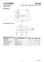
TSH190Bipolar High Voltage Hall Effect Latch Typical Application Circuit Cl : lOOOpF Output C2 ’ 15pF -O R1 : 10KQ Electrical Specifications (DC Operating Parameters : Ta=+250C,Vcc=12V)
Open the catalog to page 2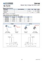
TAIWAN SEMICONDUCTOR TSH190Bipolar High Voltage Hall Effect Latch Magnetic Specifications Parameters Note: 1G (Gauss) = 0.1mT (millitesta) Output Behavior versus Magnetic Pole DC Operating Parameters: TA = -40 to 125oC, VCc = 4 to 30V OUT=Low (VDSon) OUT=Open (Pull-up Voltage)
Open the catalog to page 3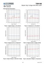
TSH190Bipolar High Voltage Hall Effect Latch Characteristic Performance Figure 2. Temperature vs. Flux Density
Open the catalog to page 4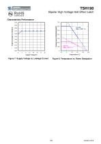
TSH190 Bipolar High Voltage Hall Effect Latch Characteristic Performance Figure 7. Supply Voltage vs. Leakage Current Figure 8. Temperature vs. Power Dissipation
Open the catalog to page 5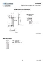
TSH190 Bipolar High Voltage Hall Effect Latch Marking Diagram 190 = Device Code Y = Year Code WW = Week Code (01~52)
Open the catalog to page 6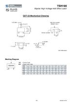
TAIWAN SEMICONDUCTOR TSH190 Bipolar High Voltage Hall Effect Latch SOT-23 Mechanical Drawing Marking Diagram 190 = Device CodeWW = Week Code Table week
Open the catalog to page 7
TSH190 Bipolar High Voltage Hall Effect Latch Notice Specifications of the products displayed herein are subject to change without notice. TSC or anyone on its behalf, assumes no responsibility or liability for any errors or inaccuracies. Information contained herein is intended to provide a product description only. No license, express or implied, to any intellectual property rights is granted by this document. Except as provided in TSC’s terms and conditions of sale for such products, TSC assumes no liability whatsoever, and disclaims any express or implied warranty, relating to sale and/or...
Open the catalog to page 8All Taiwan Semiconductor catalogs and technical brochures
 TS1117BCW50
7 Pages
 TS1117BCW33
7 Pages
 TS2937CM33
10 Pages
 TS1935BCX5
8 Pages
 TS2581CS
7 Pages
 TS2596CM5
8 Pages
 TS2596CM533
8 Pages
 TS2596CM550
8 Pages
 TS1431BCX
10 Pages
 TS431ACX-Z
10 Pages
 TS431ARCX-Z
10 Pages
 TS431ARIX-Z
7 Pages
 TS431BCX-Z
10 Pages
 TS431BRIX-Z
7 Pages
 TS432ACT
12 Pages
 TSH181CT
7 Pages
 TSH188CT
8 Pages
 TSH188CX
8 Pages
 TSH190CX
8 Pages
 TSC Web Selector Guide
43 Pages
 TS19320CS
9 Pages
 TSM015NA03CR_A1612
6 Pages
 TESD24VS2BT_A1805
5 Pages
 MCR100-3
5 Pages
 1.5KE
1.5KE6 Pages
 ABS2
ABS24 Pages
 ES1G
ES1G4 Pages
 ES1FL
ES1FL4 Pages
 ES1DL
ES1DL4 Pages
 ES1CL
ES1CL4 Pages
 ES1BL
ES1BL4 Pages
 ES1AL
ES1AL4 Pages
 ES0406D1
3 Pages
 PRODUCT SELECTOR GUIDE
27 Pages
 Product Shortform
97 Pages


Archived catalogs
 High Voltage NPN Transistor
6 Pages
 20V Dual N- Channel MOSFET
6 Pages


