- Catalogs
- Taiwan Semiconductor
- TS331CX5 Power Management Ics-Amplifier & Comparator-Comparator
TS331CX5 Power Management Ics-Amplifier & Comparator-Comparator
1 /5Pages

TS331CX5 Power Management Ics-Amplifier & Comparator-Comparator
1 /5Pages
Catalog excerpts
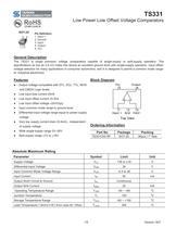
TS331 Low Power Low Offset Voltage Comparators SOT-25 Pin Definition: 1. Input + 2. Ground 3. Input 4. Output 5. Vcc General Description The TS331 is single precision voltage comparators capable of single-supply or split-supply operation. The specifications as low as 2.0 mV make this device an excellent ground level with single-supply operation. Input offsetvoltage selection for many applications in consumer automotive, and It is designed to permit a common mode rangeto- industrial electronics. Block Diagram Output voltage compatible with DTL, ECL, TTL, MOS and CMOS Logic levels Low input bias current 25nA Low input offset current ±0.5nA Low input offset voltage ±2mV(typ) Input common mode range to ground level Differential input voltage range equal to power supply voltage Very low supply current drain (0.4mA) - independent of supply voltage Wide single-supply range 2V~36V Ordering Information Part No. TS331CX5 RF Absolute Maximum Rating Parameter Supply Voltage Differential Input Voltage Input Common Mode Voltage Range Input Current Output Short Circuit to Ground Output Sink Current Operating Temperature Range Junction Temperature Storage Temperature Range Lead Temperature 1.6mm(1/16”) from case for 10Sec.
Open the catalog to page 1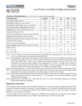
TS331 Low Power Low Offset Voltage Comparators Electrical Characteristics (VCC = 5V, Ta=25oC; unless otherwise specified.) Characteristics Input Offset Voltage (note 3) Input Offset Current, IIN(+) - IIN(-), VCM=0V Input Offset Current (note 4), IIN(+) - IIN(-), VCM=0V Input Common Mode Voltage Range, Vcc=30V Response Time (note 6), VRL=5V. RL=5.1KΩ Output Sink Current, VIN(-)=1V, VIN(+)=0V, Vo≤1.5V Large Signal Response Time Vin=TTL Logic Swing. Vref = 1.4V, VRL=5V. RL=5.1KΩ Output Saturation Voltage, VIN(-)=1V, VIN(+)=0V, ISINK≤4mA Output Leakage Current, VIN(-)=0V, VIN(+)=1V, Vo=5V Supply...
Open the catalog to page 2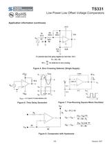
Low Power Low Offset Voltage Comparators Application information (continues) D1 prevents input from going negative by more than 0.6 V. R3< — for small error in zero crossing. Figure 4. Zero Crossing Detector (Single Supply) Vh(mfi) - 0.4 V peak for 1% phase distorton (AH). Figure 6. Time Delay Generator Figure 7. Free-Running Square-Wave Oscillator Figure 8. Comparator with Hysteresis
Open the catalog to page 3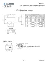
Low Power Low Offset Voltage Comparators Front View Marking Diagram (A=Jan, B=Feb, C=Mar, D=Apl, E=May, F=Jun, G=Jul, H=Aug, l=Sep, J=Oct, K=Nov, L=Dec)
Open the catalog to page 4
TS331 Low Power Low Offset Voltage Comparators Notice Specifications of the products displayed herein are subject to change without notice. TSC or anyone on its behalf, assumes no responsibility or liability for any errors or inaccuracies. Information contained herein is intended to provide a product description only. No license, express or implied, to any intellectual property rights is granted by this document. Except as provided in TSC’s terms and conditions of sale for such products, TSC assumes no liability whatsoever, and disclaims any express or implied warranty, relating to sale and/or...
Open the catalog to page 5All Taiwan Semiconductor catalogs and technical brochures
 TS1117BCW50
7 Pages
 TS1117BCW33
7 Pages
 TS2937CM33
10 Pages
 TS1935BCX5
8 Pages
 TS2581CS
7 Pages
 TS2596CM5
8 Pages
 TS2596CM533
8 Pages
 TS2596CM550
8 Pages
 TS1431BCX
10 Pages
 TS431ACX-Z
10 Pages
 TS431ARCX-Z
10 Pages
 TS431ARIX-Z
7 Pages
 TS431BCX-Z
10 Pages
 TS431BRIX-Z
7 Pages
 TS432ACT
12 Pages
 TSH181CT
7 Pages
 TSH188CT
8 Pages
 TSH188CX
8 Pages
 TSH190CT
8 Pages
 TSH190CX
8 Pages
 TSC Web Selector Guide
43 Pages
 TS19320CS
9 Pages
 TSM015NA03CR_A1612
6 Pages
 TESD24VS2BT_A1805
5 Pages
 MCR100-3
5 Pages
 1.5KE
1.5KE6 Pages
 ABS2
ABS24 Pages
 ES1G
ES1G4 Pages
 ES1FL
ES1FL4 Pages
 ES1DL
ES1DL4 Pages
 ES1CL
ES1CL4 Pages
 ES1BL
ES1BL4 Pages
 ES1AL
ES1AL4 Pages
 ES0406D1
3 Pages
 PRODUCT SELECTOR GUIDE
27 Pages
 Product Shortform
97 Pages


Archived catalogs
 High Voltage NPN Transistor
6 Pages
 20V Dual N- Channel MOSFET
6 Pages


