
- Catalogs
- Taiwan Semiconductor
- TS324 Low Power Quad Operational Amplifiers

- Products
- Catalogs
- News & Trends
- Exhibitions
TS324 Low Power Quad Operational Amplifiers

TS324 Low Power Quad Operational Amplifiers
Catalog excerpts
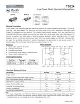
TS324 Low Power Quad Operational Amplifiers 1/8 Version: A09 DIP-14 SOP-14 General Description TS324 contains four independent high gain operational amplifiers with internal frequency compensation. The four opamps use a split power supply. The device has low power supply current drain, regardless or the power supply voltage. The low power drain also makes the TS324 a good choice for battery operation. When your project calls for a traditional op-amp function, now you can streamline your design with a simple single power supply. Use ordinary +5V common to practically any digital system or personal computer application, without requiring an extra 15V power supply just to have the interface electronics you need. TS324 is a versatile, rugged workhorse with a thousand-andone uses, from amplifying signals from a variety of transducers to dc gain blocks, or any op-amp function. The attached pages offer some recipes that will have your project cooking in no time. Absolute Maximum Rating Parameter Symbol Limit Unit Supply Voltage VCC +32 or ±16 V Differential Input Voltage (Split Power Supplies) VIDR 32 V Input Common Mode Voltage Range (note 1) VICR -0.3 to 32 V Input Forward Current (note 2) IIF 50 mA Output Short Circuit Duration TSC Continuous Operating Temperature Range TOPR 0 ~ +70 oC Junction Temperature TJ +150 oC Storage Temperature Range TSTG -65 ~ +150 oC Note: 1, For supply voltages less than 32V for the TS324 the absolute maximum input voltage is equal to the supply voltage. 2, This input current will only exist when the voltage is negative at any of the input leads. Normal output states will reestablish when the input voltage returns to a voltage greater than -0.3V. Features œ Single supply operation: 3V to 32V œ Low input bias currents œ Internally compensated œ Common mode range extends to negative supply œ Single and split supply operation Ordering Information Part No. Package Packing TS324CD14 C4 DIP-14 50pcs / Tube TS324CS14 RL SOP-14 2.5Kpcs / 13” Reel Block Diagram Pin Definition: 1. Output A 14. Output D 2. Input A (-) 13. Input D (-) 3. Input A (+) 12. Input D (+) 4. Vcc 11. Gnd 5. Input B (+) 10. Input C (+) 6. Input B (-) 9. Input C (-) 7. Output B 8. Output C
Open the catalog to page 1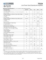
TS324 Low Power Quad Operational Amplifiers 2/8 Version: A09 Electrical Characteristics (VCC = 5V, Ta=25ºC; unless otherwise specified.) Characteristics Symbol Min Typ Max Unit Input Offset Voltage VCC= 5.0V to 30V, VIC= 0V to VCC -1.7 V, Vo= 1.4V, RS= 0Ù TLOW TA THIGH VIO -- -- 2.0 -- 7.0 9.0 mV Average Temperature Coefficient of Input Offset Voltage ÄVIO/ÄT -- 7.0 -- uV/oC Input Offset Current TA=+25ºC TLOW Ta THIGH IIO -- -- 5.0 -- 50 150 nA Average Temperature Coefficient of input Offset Current ÄIIO/ÄT -- 10 -- pA/oC Input Bias Current TA=+25ºC TLOW TA THIGH IIB -- -- -90 -- -250 -500 nA...
Open the catalog to page 2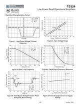
TS324 Low Power Quad Operational Amplifiers 3/8 Version: A09 Electrical Characteristics Curve Figure 1. Large Signal Voltage Follower Response Figure 2. Input Voltage Range Figure 3. Open Loop Frequency Figure 4. Large Signal Frequency Response Figure 5. Small-Signal Voltage Follower Pulse Response (Noninverting) Figure 6. Power Supply Current vs. Supply Voltage
Open the catalog to page 3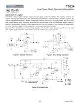
TS324 Low Power Quad Operational Amplifiers 4/8 Version: A09 Application Description The TS324 made using four internally compensated, two-stage operational amplifiers. The first stage performs not only the first stage gain function but also performs the level shifting and transconductance reduction functions. By reducing the transconductance, a smaller compensation capacitor (only 5.0pF) can be employed, thus saving chip area. Another feature of this input stage is that the input common mode range can include the negative supply or ground, in single supply operation, without saturating either...
Open the catalog to page 4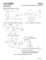
TS324 Low Power Quad Operational Amplifiers 5/8 Version: A09 Application Description (Continues) Figure 10. High Impedance Differential Amplifier Figure 11. Comparator with Hysteresis Figure 12. Function Generator Figure 13. Multiple Feedback Bandpass Filter
Open the catalog to page 5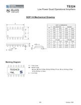
TS324 Low Power Quad Operational Amplifiers 6/8 Version: A09 SOP-14 Mechanical Drawing Marking Diagram Y = Year Code M = Month Code (A=Jan, B=Feb, C=Mar, D=Apl, E=May, F=Jun, G=Jul, H=Aug, I=Sep, J=Oct, K=Nov, L=Dec) L = Lot Code SOP-14 DIMENSION MILLIMETERS INCHES DIM MIN MAX MIN MAX A 8.55 8.75 0.337 0.344 B 3.80 4.00 0.150 0.157 C 1.35 1.75 0.054 0.068 D 0.35 0.49 0.014 0.019 F 0.40 1.25 0.016 0.049 G 1.27 (typ) 0.05 (typ) K 0.10 0.25 0.004 0.009 M 0o 7o 0o 7o P 5.80 6.20 0.229 0.244 R 0.25 0.50 0.010 0.019
Open the catalog to page 6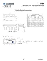
TS324 Low Power Quad Operational Amplifiers 7/8 Version: A09 DIP-14 Mechanical Drawing Marking Diagram Y = Year Code M = Month Code (A=Jan, B=Feb, C=Mar, D=Apl, E=May, F=Jun, G=Jul, H=Aug, I=Sep, J=Oct, K=Nov, L=Dec) L = Lot Code DIP-14 DIMENSION MILLIMETERS INCHES DIM MIN MAX MIN MAX A 18.55 19.56 0.730 0.770 B 6.22 6.48 0.245 0.255 C 3.18 4.45 0.125 0.135 D 0.35 0.55 0.019 0.020 G 2.54 (typ) 0.10 (typ) J 0.29 0.31 0.011 0.012 K 3.25 3.35 0.128 0.132 L 7.75 8.00 0.305 0.315 M -- 10o -- 10o
Open the catalog to page 7
TS324 Low Power Quad Operational Amplifiers 8/8 Version: A09 Notice Specifications of the products displayed herein are subject to change without notice. TSC or anyone on its behalf, assumes no responsibility or liability for any errors or inaccuracies. Information contained herein is intended to provide a product description only. No license, express or implied, to any intellectual property rights is granted by this document. Except as provided in TSC’s terms and conditions of sale for such products, TSC assumes no liability whatsoever, and disclaims any express or implied warranty, relating...
Open the catalog to page 8All Taiwan Semiconductor catalogs and technical brochures
 TS1117BCW50
7 Pages
 TS1117BCW33
7 Pages
 TS2937CM33
10 Pages
 TS1935BCX5
8 Pages
 TS2581CS
7 Pages
 TS2596CM5
8 Pages
 TS2596CM533
8 Pages
 TS2596CM550
8 Pages
 TS1431BCX
10 Pages
 TS431ACX-Z
10 Pages
 TS431ARCX-Z
10 Pages
 TS431ARIX-Z
7 Pages
 TS431BCX-Z
10 Pages
 TS431BRIX-Z
7 Pages
 TS432ACT
12 Pages
 TSH181CT
7 Pages
 TSH188CT
8 Pages
 TSH188CX
8 Pages
 TSH190CT
8 Pages
 TSH190CX
8 Pages
 TSC Web Selector Guide
43 Pages
 TS19320CS
9 Pages
 TSM015NA03CR_A1612
6 Pages
 TESD24VS2BT_A1805
5 Pages
 MCR100-3
5 Pages
 1.5KE
1.5KE6 Pages
 ABS2
ABS24 Pages
 ES1G
ES1G4 Pages
 ES1FL
ES1FL4 Pages
 ES1DL
ES1DL4 Pages
 ES1CL
ES1CL4 Pages
 ES1BL
ES1BL4 Pages
 ES1AL
ES1AL4 Pages
 ES0406D1
3 Pages
 PRODUCT SELECTOR GUIDE
27 Pages
 Product Shortform
97 Pages


Archived catalogs
 High Voltage NPN Transistor
6 Pages
 20V Dual N- Channel MOSFET
6 Pages


