- Catalogs
- Taiwan Semiconductor
- TS19371CX6 Power Management Ics-Switching Regulator-Lighting IC
TS19371CX6 Power Management Ics-Switching Regulator-Lighting IC
1 /10Pages

TS19371CX6 Power Management Ics-Switching Regulator-Lighting IC
1 /10Pages
Catalog excerpts
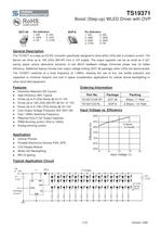
TS19371 Boost (Step-up) WLED Driver with OVP SOT-26 General Description The TS19371 is a step-up DC/DC converter specifically designed to drive white LEDs with a constant current. The device can drive up to 126 LEDs (9S14P) from a 12V supply. The output capacitor can be as small as 4.7µF, saving space versus alternative solutions. A low 95mV feedback voltage minimizes power loss for better efficiency. Additional feature include over output voltage limiting (SOT-26 package) when LEDs are disconnected. The TS19371 switches at a fixed frequency of 1.2MHz, allowing the use of tiny, low profile inductors and capacitors to minimize footprint and cost in space consideration applications for cellular phone backlighting or other hand held equipment. Inherently Matched LED Current High Efficiency: 89% Typical Drives Up to 9 LEDs Series @ Vin 9~15V Drives Up to 126 LEDs (9S14P) @ Vin 12~15V Drives Up to 6 (1W) LEDs Series @ Vin 12V Over Output Voltage Protection 30V (SOT-26) Fast 1.2MHz Switching Frequency Requires Only 4.7µF Output Capacitor PWM dimming control 1KHz to 10KHz Analog dimming control Ordering Information Part No. Input Voltage vs. Efficiency Cellular Phones Portable Electronics Devices PDA, GPS Typical Application Circuit
Open the catalog to page 1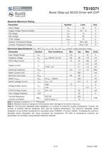
TS19371 Boost (Step-up) WLED Driver with OVP Absolute Maximum Rating Parameter Supply Voltage (Recommended) Input Voltage CTRL Voltage Ambient Temperature Range Junction Temperature Range Electrical Specifications (Ta = 25oC, VIN= VCTRL=3V, CIN=1uF, COUT=0.22uF unless otherwise noted) Parameter Input Voltage Range FB Pin Bias Current Supply Current Feedback Voltage Test Conditions Switching Frequency Switch Current Limit Maximum Duty Cycle Switch VCESAT Switch Leakage Current Voltage Enable Control CTRL Pin Bias Current Over Voltage Protection Thermal Resistance - ° C/W Junction to Ambient SOP-8...
Open the catalog to page 2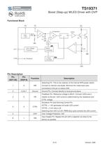
TS19371 Boost (Step-up) WLED Driver with OVP Functional Block Description Switching Pin. This is the collector of the internal NPN power switch. Connect to inductor and diode. Minimize the metal trace area connected to this pin to reduce EMI. Ground Pin. Connect directly to local ground plane. Feedback Pin. Reference voltage is 95mV. Connect LEDs and a resistor at this pin. LED current is determined by the resistance and CTRL voltage. Shutdown Pin and Dimming Control Pin. VCTRL > 1.8V generates full-scale LED current VCTRL < 0.4V chip is off Switching from 04V to 2.0V, PWM duty cycle controls...
Open the catalog to page 3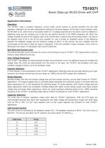
TS19371 Boost (Step-up) WLED Driver with OVP Application Information Operation The TS19371 uses a constant frequency, current mode control scheme to provide excellent line and load regulation. Operation can be best understood by referring to the block diagram. At the start of each oscillator cycle, the RS latch is set, which turns on the power switch Q1. A voltage proportional to the switch current is added to a stabilizing ramp and the resulting sum is fed into the positive terminal of the PWM comparator A2. When this voltage exceeds the level at the negative input of A2, the RS latch is reset...
Open the catalog to page 4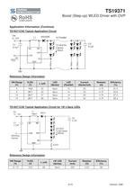
TS19371 Boost (Step-up) WLED Driver with OVP Application Information (Continue) TS19371CX6 Typical Application Circuit Reference Design Information VIN Range (V) Current (Series/mA) TS19371CX6 Typical Application Circuit for 1W x 6pcs LEDs Reference Design Information VIN Range (V)
Open the catalog to page 5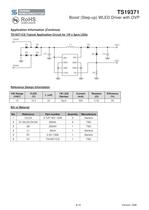
TS19371 Boost (Step-up) WLED Driver with OVP Application Information (Continue) TS19371CS Typical Application Circuit for 1W x 5pcs LEDs Reference Design Information VIN Range (VAC) Manufacture Generic
Open the catalog to page 6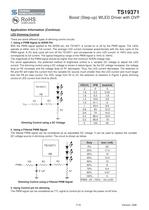
TS19371 Boost (Step-up) WLED Driver with OVP Application Information (Continue) LED Dimming Control There are some different types of dimming control circuits: 1. Using a PWM Signal to SHDN Pin With the PWM signal applied to the SHDN pin, the TS19371 is turned on or off by the PWM signal. The LEDs operate at either zero or full current. The average LED current increases proportionally with the duty cycle of the PWM signal. A 0% duty cycle will turn off the TS19371 and corresponds to zero LED current. A 100% duty cycle corresponds to full current. The typical frequency range of the PWM signal...
Open the catalog to page 7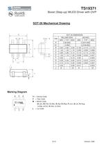
TS19371 Boost (Step-up) WLED Driver with OVP Marking Diagram 71 = Device Code Y = Year Code M = Month Code (A=Jan, B=Feb, C=Mar, D=Apl, E=May, F=Jun, G=Jul, H=Aug, I=Sep, J=Oct, K=Nov, L=Dec) L = Lot Code
Open the catalog to page 8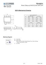
TS19371 Boost (Step-up) WLED Driver with OVP Marking Diagram Y = Year Code M = Month Code (A=Jan, B=Feb, C=Mar, D=Apl, E=May, F=Jun, G=Jul, H=Aug, I=Sep, J=Oct, K=Nov, L=Dec) L = Lot Code
Open the catalog to page 9
TS19371 Boost (Step-up) WLED Driver with OVP Notice Specifications of the products displayed herein are subject to change without notice. TSC or anyone on its behalf, assumes no responsibility or liability for any errors or inaccuracies. Information contained herein is intended to provide a product description only. No license, express or implied, to any intellectual property rights is granted by this document. Except as provided in TSC’s terms and conditions of sale for such products, TSC assumes no liability whatsoever, and disclaims any express or implied warranty, relating to sale and/or...
Open the catalog to page 10All Taiwan Semiconductor catalogs and technical brochures
 TS1117BCW50
7 Pages
 TS1117BCW33
7 Pages
 TS2937CM33
10 Pages
 TS1935BCX5
8 Pages
 TS2581CS
7 Pages
 TS2596CM5
8 Pages
 TS2596CM533
8 Pages
 TS2596CM550
8 Pages
 TS1431BCX
10 Pages
 TS431ACX-Z
10 Pages
 TS431ARCX-Z
10 Pages
 TS431ARIX-Z
7 Pages
 TS431BCX-Z
10 Pages
 TS431BRIX-Z
7 Pages
 TS432ACT
12 Pages
 TSH181CT
7 Pages
 TSH188CT
8 Pages
 TSH188CX
8 Pages
 TSH190CT
8 Pages
 TSH190CX
8 Pages
 TSC Web Selector Guide
43 Pages
 TS19320CS
9 Pages
 TSM015NA03CR_A1612
6 Pages
 TESD24VS2BT_A1805
5 Pages
 MCR100-3
5 Pages
 1.5KE
1.5KE6 Pages
 ABS2
ABS24 Pages
 ES1G
ES1G4 Pages
 ES1FL
ES1FL4 Pages
 ES1DL
ES1DL4 Pages
 ES1CL
ES1CL4 Pages
 ES1BL
ES1BL4 Pages
 ES1AL
ES1AL4 Pages
 ES0406D1
3 Pages
 PRODUCT SELECTOR GUIDE
27 Pages
 Product Shortform
97 Pages


Archived catalogs
 High Voltage NPN Transistor
6 Pages
 20V Dual N- Channel MOSFET
6 Pages


