- Catalogs
- Taiwan Semiconductor
- TS1935BCX5
TS1935BCX5
1 /8Pages

TS1935BCX5
1 /8Pages
Catalog excerpts
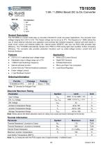
TS1935B1.9A / 1.2MHz Boost DC to Dc Converter Pin Defi nition: General Description The TS1935B is a current mode step up converter intended for small, low power applications. The converter input voltage ranging from 2.6V to 5.5V. The Output voltage can be set up to 27V. The frequency is 1.2MHz allows the use of small external inductors and capacitors and provides fast transient response. Internal soft start results in small inrush current and extends battery life. Internal power MOSFET with very low RDS (ON) provides high efficiency. The TS1935B automatically transits from PWM to PFM during light load condition further increasing efficiency. The converter also provides protection functions such as under-voltage lockout, current limit and thermal shutdown. Application • White LED Current Source • Digital Still Cameras • Portable Electronics • PDA’s and Palm-Top Computers • Local Boost Regulator Features • 2.6V to 5.5 V operating input voltage range • Adjustable output voltage range up to 27V • 1.2MHz Fixed Switching Frequency • Internal soft-start function • Current limit and Thermal shutdown protection • Under voltage Lockout • < 1^A Shutdown Current Note: Stress above the listed absolute maximum rating may cause permanent damage to the device Thermal Information
Open the catalog to page 1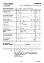
TS1935B1.9A / 1.2MHz Boost DC to Dc Converter Electrical Specifications (Ta = 25oC, VIN=5V, Note 1: Guaranteed by design Pin Description
Open the catalog to page 2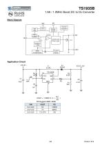
TS1935B 1.9A / 1.2MHz Boost DC to Dc Converter Block Diagram EN Soft Start Thermal Shutdown Enable/ Disable Summing Comparator SW Control and Driver Logic Error Amplifier Current Sense Slope Compensation
Open the catalog to page 3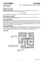
TS1935B 1.9A / 1.2MHz Boost DC to Dc Converter Application Information Setting the Output Voltage Application circuit item shows the basic application circuit with AX5511 adjustable output version. The external resistor sets the output voltage according to the following equation: R2 VOUT = 1.238V × (1+ ) R1 For most applications, R2 is a suggested a value by 390K~820KΩ. Place the resistor-divider as close to the IC as possible to reduce the noise sensitivity. Under Voltage Lockout (UVLO) To avoid mis-operation of the device at low input voltages an under voltage lockout is included that disables...
Open the catalog to page 4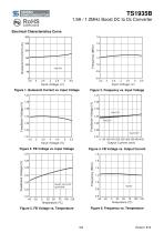
TS1935B 1.9A / 1.2MHz Boost DC to Dc Converter Electrical Characteristics Curve Figure 1. Quiescent Current vs. Input Voltage Figure 2. Frequency vs. Input Voltage Figure 3. FB Voltage vs. Input Voltage Figure 4. FB Voltage vs. Output Current Figure 5. FB Voltage vs. Temperature Figure 6. Frequency vs. Temperature
Open the catalog to page 5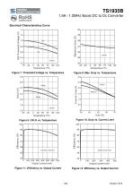
TS1935B1.9A / 1.2MHz Boost DC to Dc Converter COMPLIANCE Electrical Characteristics Curve 1.4 > V1-2 Q) 03 r° T3 o 0.8 Figure 11. Efficiency vs. Output Current Figure 12. Efficiency vs. Output Current
Open the catalog to page 6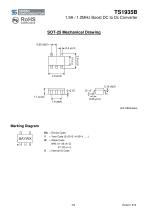
TAIWAN SEMICONDUCTOR SOT-25 Mechanical Drawing Unit: Millimeters W = Week Code WW: 01~26 (A~Z) 27~52 (a~z) X = Internal ID Code
Open the catalog to page 7
Notice Specifications of the products displayed herein are subject to change without notice. TSC or anyone on its behalf, assumes no responsibility or liability for any errors or inaccuracies. Information contained herein is intended to provide a product description only. No license, express or implied, to any intellectual property rights is granted by this document. Except as provided in TSC’s terms and conditions of sale for such products, TSC assumes no liability whatsoever, and disclaims any express or implied warranty, relating to sale and/or use of TSC products including liability or warranties...
Open the catalog to page 8All Taiwan Semiconductor catalogs and technical brochures
 TS1117BCW50
7 Pages
 TS1117BCW33
7 Pages
 TS2937CM33
10 Pages
 TS2581CS
7 Pages
 TS2596CM5
8 Pages
 TS2596CM533
8 Pages
 TS2596CM550
8 Pages
 TS1431BCX
10 Pages
 TS431ACX-Z
10 Pages
 TS431ARCX-Z
10 Pages
 TS431ARIX-Z
7 Pages
 TS431BCX-Z
10 Pages
 TS431BRIX-Z
7 Pages
 TS432ACT
12 Pages
 TSH181CT
7 Pages
 TSH188CT
8 Pages
 TSH188CX
8 Pages
 TSH190CT
8 Pages
 TSH190CX
8 Pages
 TSC Web Selector Guide
43 Pages
 TS19320CS
9 Pages
 TSM015NA03CR_A1612
6 Pages
 TESD24VS2BT_A1805
5 Pages
 MCR100-3
5 Pages
 1.5KE
1.5KE6 Pages
 ABS2
ABS24 Pages
 ES1G
ES1G4 Pages
 ES1FL
ES1FL4 Pages
 ES1DL
ES1DL4 Pages
 ES1CL
ES1CL4 Pages
 ES1BL
ES1BL4 Pages
 ES1AL
ES1AL4 Pages
 ES0406D1
3 Pages
 PRODUCT SELECTOR GUIDE
27 Pages
 Product Shortform
97 Pages


Archived catalogs
 High Voltage NPN Transistor
6 Pages
 20V Dual N- Channel MOSFET
6 Pages


