- Catalogs
- Taiwan Semiconductor
- TS19320CS
TS19320CS
1 /9Pages

TS19320CS
1 /9Pages
Catalog excerpts
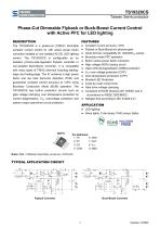
Phase-Cut Dimmable Flyback or Buck-Boost Current Control with Active PFC for LED lighting DESCRIPTION The TS19320CS is a phase-cut (TRIAC) dimmable Constant current accuracy <±5% Flyback or Buck-Boost w/o photocoupler Good dimmer compatibility for 120/230VAC Lamps Boundary-mode PFC operation Built-in active power factor correction High voltage (500V) startup circuit Open-LED demagnetization (DMG) protection VCC over-voltage protection (OVP) Over-temperature protection (OTP) Shorted-LED Protection Cycle-by-cycle current limit Gate drive voltage clamping Compliant to RoHS Directive 2011/65/EU and in accordance to WEEE 2002/96/EC. ● Halogen-free according to IEC 61249-2-21 constant current control IC with active power factor correction isolated or non-isolated AC-DC LED lighting control. The TS19320CS is configurable as an isolated, primary-side-regulated Flyback controller or non-isolated Buck-Boost converter. It is compatible with many types of TRIAC dimmers including leadingedge and trailing-edge. The IC achieves a high power factor and low total harmonic distortion (THD) and guarantees constant current accuracy to <±5% using Boundary Conduction Mode (BCM) operation. The TS19320CS has built-in protection circuits such as gate voltage clamping, over temperature protection by current degeneration, VCC overvoltage protection and system output open/short circuit protection. APPLICATION ● LED lighting ● Down lights, Tube lamps, PAR Lamps, Bulbs Notes: MSL 3 (Moisture Sensitivity Level) per J-STD-020 TYPICAL APPLICATION CIRCUIT Flyback Converter
Open the catalog to page 1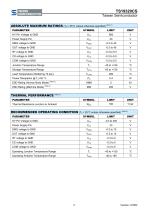
TAIWAN SEMICONDUCTOR TS19320CSTaiwan Semiconductor ABSOLUTE MAXIMUM RATINGS (TA = 25°C unless otherwise specified) (Note 11 THERMAL PERFORMANCE (Note 3) RECOMMENDED OPERATING CONDITION
Open the catalog to page 2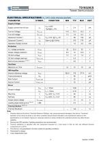
TAIWAN SEMICONDUCTOR TS19320CSTaiwan Semiconductor ELECTRICAL SPECIFICATIONS (TA = 25°C unless otherwise specified) Note: 1. Stresses listed as the above “Absolute Maximum Ratings” may cause permanent damage to the device. Functional operation of the device at these or any other conditions beyond those indicated in the operational sections of the specifications is not implied. Exposure to absolute maximum rating conditions for extended periods may affect device reliability. 2. Devices are ESD sensitive. Handling precautions are recommended. 3. Thermal resistance is specified with the component...
Open the catalog to page 3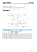
TS19320CS Taiwan Semiconductor ORDERING INFORMATION PART NO. Gate Driver Sample & Hold Angle Detection Sample & Hold set_dmg Line Compensation Pull high to line voltage for startup Maximum on time setting Input current sense pin. Output pin of error amplifier. Zero current demagnetization sensing. Power supply pin for all internal circuitry. Ground return for all internal circuitry.
Open the catalog to page 4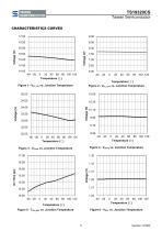
TS19320CS Taiwan Semiconductor CHARACTERISTICS CURVES Temperature (℃) Figure 2 - VCC_OFF vs. Junction Temperature Figure 1 - VCC_ON vs. Junction Temperature 35.00 Figure 4 - VOVPS vs. Junction Temperature Figure 3 - VOVPA vs. Junction Temperature Temperature (℃) Figure 5 - TON_MAX vs. Junction Temperature Figure 6 - VOCP vs. Junction Temperature
Open the catalog to page 5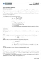
TAIWAN SEMICONDUCTOR TS19320CSTaiwan Semiconductor APPLICATION INFORMATION PSR Function Description As a constant current primary-side controller with phase-cut dimmable and PFC function for LED lighting applications, the controller operates in boundary conduction mode (BCM) with constant on-time based regulation designed to achieve high power factor performance. The TS19320 has built-in high voltage (500V) startup circuit, VCC over voltage protection, open LED protection, short LED protection, over temperature protection, primary-side current limit, and gate clamp function. The average output...
Open the catalog to page 6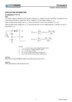
TAIWAN SEMICONDUCTOR TS19320CSTaiwan Semiconductor APPLICATION INFORMATION Pin Definitions (Continue) DMG The Output voltage is reflected by the auxiliary winding (NAUX) voltage of fly-back transformer, the DMG pin can sense output information to depart from start up voltage (Vo_stR) and protect voltage (Vo_ovp). When the DMG sense voltage under VO_STR, the circuit will work on short circuit protection, fSTR=1/tSTR. When the DMG sense voltage over VO_OVP, the circuit will work on over voltage protection, it will latch out until VCC goes below Vcc_off- Nsec Rdi + Rd2 VO OVP = x Vovps x Where...
Open the catalog to page 7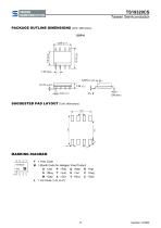
TAIWAN SEMICONDUCTOR TS19320CSTaiwan Semiconductor PACKAGE OUTLINE DIMENSIONS (Unit: Millimeters) SOP-8 SUGGESTED PAD LAYOUT (Unit: Millimeters) MARKING DIAGRAM Y = Year Code M = Month Code for Halogen Free Product
Open the catalog to page 8
Notice Specifications of the products displayed herein are subject to change without notice. TSC or anyone on its behalf, assumes no responsibility or liability for any errors or inaccuracies. Information contained herein is intended to provide a product description only. No license, express or implied, to any intellectual property rights is granted by this document. Except as provided in TSC’s terms and conditions of sale for such products, TSC assumes no liability whatsoever, and disclaims any express or implied warranty, relating to sale and/or use of TSC products including liability or warranties...
Open the catalog to page 9All Taiwan Semiconductor catalogs and technical brochures
 TS1117BCW50
7 Pages
 TS1117BCW33
7 Pages
 TS2937CM33
10 Pages
 TS1935BCX5
8 Pages
 TS2581CS
7 Pages
 TS2596CM5
8 Pages
 TS2596CM533
8 Pages
 TS2596CM550
8 Pages
 TS1431BCX
10 Pages
 TS431ACX-Z
10 Pages
 TS431ARCX-Z
10 Pages
 TS431ARIX-Z
7 Pages
 TS431BCX-Z
10 Pages
 TS431BRIX-Z
7 Pages
 TS432ACT
12 Pages
 TSH181CT
7 Pages
 TSH188CT
8 Pages
 TSH188CX
8 Pages
 TSH190CT
8 Pages
 TSH190CX
8 Pages
 TSC Web Selector Guide
43 Pages
 TSM015NA03CR_A1612
6 Pages
 TESD24VS2BT_A1805
5 Pages
 MCR100-3
5 Pages
 1.5KE
1.5KE6 Pages
 ABS2
ABS24 Pages
 ES1G
ES1G4 Pages
 ES1FL
ES1FL4 Pages
 ES1DL
ES1DL4 Pages
 ES1CL
ES1CL4 Pages
 ES1BL
ES1BL4 Pages
 ES1AL
ES1AL4 Pages
 ES0406D1
3 Pages
 PRODUCT SELECTOR GUIDE
27 Pages
 Product Shortform
97 Pages


Archived catalogs
 High Voltage NPN Transistor
6 Pages
 20V Dual N- Channel MOSFET
6 Pages


