- Catalogs
- Taiwan Semiconductor
- TS1117BCW50
TS1117BCW50
1 /7Pages

TS1117BCW50
1 /7Pages
Catalog excerpts

TAIWAN SEMICONDUCTOR TS1117B Series Taiwan Semiconductor 1A Low Dropout Positive Voltage Regulator DESCRIPTION TS1117B are high performance positive voltage regulators are designed for use in applications requiring low dropout performance at full rated current. Additionally; TS1117B provides excellent regulation over variations due to changes in line, load and temperature. Outstanding features include low dropout performance at rated current, fast transient response, internal current limiting and thermal shutdown protection of the output device. TS1117B are three terminal regulators with fixed and adjustable voltage options available in popular packages. FEATURES • Low Dropout Performance 1.5V max. • Fast T ransient Response • Built-in thermal shutdown • Output Current Limit • Line Regulation Typical 0.2% • Load Regulation Typical 0.05% • Low-ESR Ceramic Capacitor (MLCC) required for Stability. • Good Ripple Rejection • Compliant to RoHS Directive 2011/65/EU and WEEE 2002/96/EC • Halogen-free according to IEC 61249-2-21 APPLICATION • PC peripheral • Communication • Consumer equipment HALOGEN FREE Pb-Free COMPLIANT Notes: MSL 3 (Moisture Sensitivity Level) per J-STD-020 TYPICAL APPLICATION CIRCUIT Fixed output voltage version
Open the catalog to page 1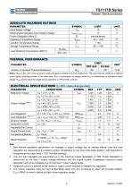
TAIWAN SEMICONDUCTOR TS1117B SeriesTaiwan Semiconductor ABSOLUTE MAXIMUM RATINGS Notes: R©ja is the sum of the junction-to-case and case-to-ambient thermal resistances. The case thermal reference is defined at the solder mounting surface of the drain pins. R©ja is guaranteed by design while R©ca is determined by the user’s board design. R©ja shown below for single device operation on FR-4 PCB in still air. 1. See thermal regulation specification for changes in output voltage due to heating effects. Line and load regulation are measured at a constant junction temperature by low duty cycle pulse...
Open the catalog to page 2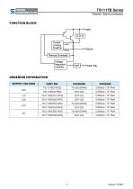
TAIWAN SEMICONDUCTOR TS1117B SeriesTaiwan Semiconductor FUNCTION BLOCK ORDERING INFORMATION Input Current Output Thermal Overload Voltage Regulation Amplifier Vref —o Fixed/Adj OUTPUT VOLTAGE
Open the catalog to page 3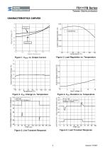
TAIWAN SEMICONDUCTOR TS1117B SeriesTaiwan SemiconductorCHARACTERISTICS CURVES o > TIME (US) Figure 5. Line Transient Response
Open the catalog to page 4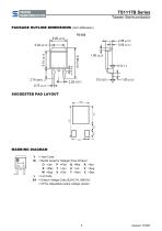
TAIWAN SEMICONDUCTOR TS1117B SeriesTaiwan Semiconductor SUGGESTED PAD LAYOUT MARKING DIAGRAM Y = Year Code M = Month Code for Halogen Free Product O =Jan P =Feb Q =Mar R =Apr L = Lot Code XX = Output Voltage Code (3.3=3.3V, 5.0=5V) = CP for Adjustable output voltage version
Open the catalog to page 5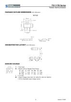
TAIWAN SEMICONDUCTOR TS1117B SeriesTaiwan Semiconductor PACKAGE OUTLINE DIMENSIONS (Unit: Millimeters) SOT-223 SUGGESTED PAD LAYOUT (Unit: Millimeters) MARKING DIAGRAM Y = Year Code M = Month Code for Halogen Free Product O =Jan P =Feb Q =Mar R =Apr L = Lot Code XX = Output Voltage Code (1.2=1.2V, 2.5=2.5V, 3.3=3.3V, 5.0=5V) = CW for Adjustable output voltage version
Open the catalog to page 6
TS1117B Series Taiwan Semiconductor Notice Specifications of the products displayed herein are subject to change without notice. TSC or anyone on its behalf, assumes no responsibility or liability for any errors or inaccuracies. Information contained herein is intended to provide a product description only. No license, express or implied, to any intellectual property rights is granted by this document. Except as provided in TSC’s terms and conditions of sale for such products, TSC assumes no liability whatsoever, and disclaims any express or implied warranty, relating to sale and/or use of TSC...
Open the catalog to page 7All Taiwan Semiconductor catalogs and technical brochures
 TS1117BCW33
7 Pages
 TS2937CM33
10 Pages
 TS1935BCX5
8 Pages
 TS2581CS
7 Pages
 TS2596CM5
8 Pages
 TS2596CM533
8 Pages
 TS2596CM550
8 Pages
 TS1431BCX
10 Pages
 TS431ACX-Z
10 Pages
 TS431ARCX-Z
10 Pages
 TS431ARIX-Z
7 Pages
 TS431BCX-Z
10 Pages
 TS431BRIX-Z
7 Pages
 TS432ACT
12 Pages
 TSH181CT
7 Pages
 TSH188CT
8 Pages
 TSH188CX
8 Pages
 TSH190CT
8 Pages
 TSH190CX
8 Pages
 TSC Web Selector Guide
43 Pages
 TS19320CS
9 Pages
 TSM015NA03CR_A1612
6 Pages
 TESD24VS2BT_A1805
5 Pages
 MCR100-3
5 Pages
 1.5KE
1.5KE6 Pages
 ABS2
ABS24 Pages
 ES1G
ES1G4 Pages
 ES1FL
ES1FL4 Pages
 ES1DL
ES1DL4 Pages
 ES1CL
ES1CL4 Pages
 ES1BL
ES1BL4 Pages
 ES1AL
ES1AL4 Pages
 ES0406D1
3 Pages
 PRODUCT SELECTOR GUIDE
27 Pages
 Product Shortform
97 Pages


Archived catalogs
 High Voltage NPN Transistor
6 Pages
 20V Dual N- Channel MOSFET
6 Pages


