- Catalogs
- Taiwan Semiconductor
- B0520LW Discrete Devices-Diode-Schottky Diode & Array
B0520LW Discrete Devices-Diode-Schottky Diode & Array
1 /3Pages

B0520LW Discrete Devices-Diode-Schottky Diode & Array
1 /3Pages
Catalog excerpts

B0520LW,B0530W,B0540W 410mW, Low VF SMD Schottky Barrier Diode Small Signal Diode SOD-123 Features Low power loss, high current capability, low VF Surface device type mounting Moisture sensitivity level 1 Matte Tin(Sn) lead finish with Nickel(Ni) underplate Pb free version and RoHS compliant Green compound (Halogen free) with suffix "G" on packing code and prefix "G" on date code Dimensions Mechanical Data Unit (inch) Case : SOD-123 small outline plastic package Terminal: Matte tin plated, lead free., solderable per MIL-STD-202, Method 208 guaranteed High temperature soldering guaranteed: 260°C/10s Polarity : Indicated by cathode band Weight :0.01 gram (approximately) 0.5A surface mount schottky barrier rectifier Ordering Information Packing 3K / 7" Reel Maximum Ratings and Electrical Characteristics Rating at 25°C ambient temperature unless otherwise specified. Maximum Ratings Type Number Power Dissipation Reverse Voltage Mean Forward Current @ TL=100°C (Lead Temperature) Repetitive Peak Reverse Voltage Non-Repetitive Peak Forward Surge Current (Note 1) Thermal Resistance (Junction to Ambient) (Note 2) Junction and Storage Temperature Range Notes:1. Test Condition : 8.3ms Single half Sine-Wave Superimposed on Rated Load (JEDEC Method) Notes:2. Valid provided that electrodes are kept at ambient temperature Version : D10
Open the catalog to page 1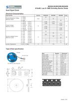
B0520LW,B0530W,B0540W 410mW, Low VF SMD Schottky Barrier Diode Small Signal Diode Electrical Characteristics Type Number Forward Voltage (Maximum value) Junction Capacitance Reverse Leakage Current (Maximum value) Reverse Breakdown Voltage (Minimum value) Tape & Reel specification TSC label Top Cover Tape Carieer Tape Any Additional Label (If Required) Item Carrier width Carrier length Carrier depth Sprocket hole Reel outside diameter Reel inner diameter Feed hole width Sprocke hole position Punch hole position Sprocke hole pitch Embossment center Overall tape thickness Tape width Reel width
Open the catalog to page 2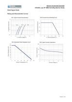
B0520LW,B0530W,B0540W 410mW, Low VF SMD Schottky Barrier Diode Small Signal Diode Rating and Sharacteristic Curves FIG 2 Forward Current Derating Curve FIG 1 Typical Forward Characteristics 1 Io mean forward current (A) FIG 3 Admissible Power Dissipation Curve FIG 4 Typical Junction Capacitance Junction Capacitance(pF)
Open the catalog to page 3All Taiwan Semiconductor catalogs and technical brochures
 TS1117BCW50
7 Pages
 TS1117BCW33
7 Pages
 TS2937CM33
10 Pages
 TS1935BCX5
8 Pages
 TS2581CS
7 Pages
 TS2596CM5
8 Pages
 TS2596CM533
8 Pages
 TS2596CM550
8 Pages
 TS1431BCX
10 Pages
 TS431ACX-Z
10 Pages
 TS431ARCX-Z
10 Pages
 TS431ARIX-Z
7 Pages
 TS431BCX-Z
10 Pages
 TS431BRIX-Z
7 Pages
 TS432ACT
12 Pages
 TSH181CT
7 Pages
 TSH188CT
8 Pages
 TSH188CX
8 Pages
 TSH190CT
8 Pages
 TSH190CX
8 Pages
 TSC Web Selector Guide
43 Pages
 TS19320CS
9 Pages
 TSM015NA03CR_A1612
6 Pages
 TESD24VS2BT_A1805
5 Pages
 MCR100-3
5 Pages
 1.5KE
1.5KE6 Pages
 ABS2
ABS24 Pages
 ES1G
ES1G4 Pages
 ES1FL
ES1FL4 Pages
 ES1DL
ES1DL4 Pages
 ES1CL
ES1CL4 Pages
 ES1BL
ES1BL4 Pages
 ES1AL
ES1AL4 Pages
 ES0406D1
3 Pages
 PRODUCT SELECTOR GUIDE
27 Pages
 Product Shortform
97 Pages


Archived catalogs
 High Voltage NPN Transistor
6 Pages
 20V Dual N- Channel MOSFET
6 Pages


