MQFL-28VE-1R5S
1 /15Pages

MQFL-28VE-1R5S
1 /15Pages
Catalog excerpts

H igH R eliability DC-DC C onveRteR 5.5-80V Continuous Input Transient Input The MilQor@ series of high-reliability DC-DC converters brings SynQor’s field proven high-efficiency synchronous rectifier technology to the Military/Aerospace industry. SynQor’s innovative QorSealTM packaging approach ensures survivability in the most hostile environments. Compatible with the industry standard format, these converters operate at a fixed frequency, have no opto-isolators, and follow conservative component derating guidelines. ILITY STAB designed and manufactured to comply with a wide range of military standards. Meets all -704 and -1275D under-voltage transients Design Process MQFL series converters are: • Designed for reliability per NAVSO-P3641-A guidelines • Designed with components derated per: — MIL-HDBK-1547A — NAVSO P-3641A Qualification Process MQFL series converters are qualified to: • MIL-STD-810F — consistent with RTCA/D0-160E • SynQor’s First Article Qualification — consistent with MIL-STD-883F • SynQor’s Long-Term Storage Survivability Qualification • SynQor’s on-going life test In-Line Manufacturing Process • AS9100 and ISO 9001:2008 certified facility • Full component traceability • Temperature cycling • Constant acceleration • 24, 96, 160 hour burn-in • Three level temperature screening DesigneD & ManufactureD in the usa featuring Qorseal™ hi-rel asseMbly Fixed switching frequency No opto-isolators Parallel operation with current share Remote sense Clock synchronization Primary and secondary referenced enable Continuous short circuit and overload protection Input under-voltage and over-voltage shutdown Specification Compliance MQFL series converters (with MQME filter) are designed to meet: • MIL-HDBK-704-8 (A through F) • RTCA/DO-160 Section 16, 17, 18 • MIL-STD-1275 (B, D) • DEF-STAN 61-5 (part 6)/(5, 6) • MIL-STD-461 (C, D, E, F) • RTCA/DO-160(E, F, G)
Open the catalog to page 1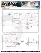
Technical Specification BLOCK DIAGRAM INPUT RETURN CURRENT SENSE ISOLATION STAGE GATE DRIVERS GATE DRIVERS OUTPUT RETURN CURRENT LIMIT REGULATION STAGE BOOST CONVERTER SWITCHES AND CONTROL ISOLATION BARRIER PRIMARY CONTROL SECONDARY CONTROL DATA COUPLING BIAS POWER CONTROL POWER TYPICAL CONNECTION DIAGRAM External bulk capacitor
Open the catalog to page 2
Technical Specification Under-Voltage Transient Profile Boost-Converter is armed (or re-armed) when Vin exceeds this value Boost-Converter Operational Area Under-Voltage Transient Profile showing when the boost-converter is guaranteed to be operational. Before the boost converter will operate, it must first be armed (or re-armed) by making VIN greater than VARM. Note: This Under-Voltage Transient Profile is designed to comply (with appropriate margins) with all initial-engagement surges, starting or cranking voltage transients and under-voltage surges specified in: • MIL-STD-704-8 (A through...
Open the catalog to page 3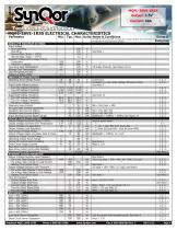
hmQcaQ SpecQGOCat MQFL-28VE-1R5S ELECTRICAL CHARACTERISTICS Parameter Group AE Subgroup ABSOLUTE MAXIMUM RATINGS Min. Typ. Max. Units Notes & Conditions Vin=28V dc ±5%, Iout=40A, CL=0pF, free running (see Note 10) boost-converter non-operational unless otherwise specified DYNAMIC CHARACTERISTICS Output Voltage Deviation Load Transient
Open the catalog to page 4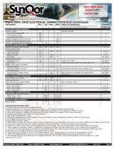
hmQcaQ SpecQGOCat MQFL-28VE-1R5S ELECT Parameter Electrical Characteristics Notes 1. Converter will undergo input over-voltage shutdown. 2. Derate output power for continuous operation per Figure 5. 135°C is above specified operating range. 3. High or low state of input voltage must persist for about 200ps to be acted on by the lockout or shutdown circuitry. 4. Current limit inception is defined as the point where the output voltage has dropped to 90% of its nominal value. 5. Parameter not tested but guaranteed to the limit specified. 6. Load current transition time > 10ps. 7. Settling time measured...
Open the catalog to page 5
Application Section BASIC OPERATION AND FEATURES The MQFL converter’s control circuit does not implement an output over-voltage limit or an over-temperature shutdown. The MQFL DC/DC converter uses a two-stage power conversion topology. The first, or regulation, stage is a buck-converter that keeps the output voltage constant over variations in line, load, and temperature. The second, or isolation, stage uses transformers to provide the functions of input/output isolation and voltage transformation to achieve the output voltage required. condition). When a load fault is removed, the output voltage...
Open the catalog to page 6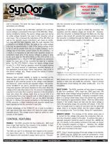
Application Section mits the converter to be inhibited from either the input or the output side. Usually the converter has an EMI filter upstream of it, and the source voltage is connected to the input of this EMI filter. When, during compliance testing, the source voltage goes low during an under-voltage transient, the input to the converter will go even lower. This is because the inductance of the EMI filter (as well as the parasitic source inductance) will cause an oscillatory ring with the bulk capacitor. With the bulk capacitor that is present in an MQME-28 filter, the peak of this under-voltage...
Open the catalog to page 7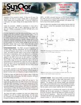
Application Section NOTE: An MQFL converter that has its SYNC IN pin driven by the SYNC OUT pin of a second MQFL converter will have its start of its switching cycle delayed approximately 180 degrees relative to that of the second converter. Figure B shows the equivalent circuit looking into the SYNC IN pin. Figure C shows the equivalent circuit looking into the SYNC OUT pin. regulation of the converter’s output. If they are left open, the converter will have an output voltage that is approximately 200mV higher than its specified value. If only the +SENSE pin is left open, the output voltage...
Open the catalog to page 8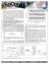
Application Section Trim Resistance (ohms) Whether or not converters are paralleled, the voltage at the SHARE pin could be used to monitor the approximate average current delivered by the converter(s). A nominal voltage of 1.0V represents zero current and a nominal voltage of 2.2V represents the maximum rated current, with a linear relationship in between. The internal source resistance of a converter’s SHARE pin signal is 2.5 kW. During an input voltage fault or primary disable event, the SHARE pin outputs a power failure warning pulse. The SHARE pin will go to 3V for approximately 14ms as the...
Open the catalog to page 9All SYNQOR catalogs and technical brochures
 SynQor
108 Pages
 VPX
VPX6 Pages
 UPS MS 1500
6 Pages
 MQFL-270L-05S
19 Pages
 MQFL-28V-1R5S
17 Pages
 MQFL-28E-1R5S
19 Pages
 MQFL-28-1R5S
19 Pages
 PQ60012SMx25
15 Pages
 PQ60 series
14 Pages
 PQ40 Series
16 Pages
 PQ30 series
14 Pages
 PQ24018QGx25
16 Pages
 SUMMER 2011 Product Catalog
52 Pages
 MilQor Mil-COTS Brochure
6 Pages
 MilQor Hi-Rel Brochure
6 Pages
- Power supply unit
- DC power supply
- AC/DC power supply
- Single-output power supply
- Electronic filter
- Passive electronic filter
- Multiple-output power supply
- Single-output DC/DC converter module
- AC electronic filter
- Isolated DC-DC converter
- Low-pass electronic filter
- Industrial DC/DC converter module
- SMD DC-DC converter
- Power supply for medical applications
- Three-phase electronic filter
- Rugged DC/DC converter
- Panel-mount power supply
- Dual-output DC/DC converter module