TSX923
1 /32Pages

TSX923
1 /32Pages
Catalog excerpts

TSX920, TSX921, TSX922, TSX92310 MHz rail-to-rail CMOS 16 V operational amplifiers Datasheet - production data Features • Rail-to-rail input and output • Wide supply voltage: 4 V - 16 V • Gain bandwidth product: 10 MHztyp at 16 V • Low power consumption: 2.8 mA typ per amplifier at 16 V • Unity gain stable • Low input bias current: 10 pA typ • High tolerance to ESD: 4 kV HBM • Extended temperature range: -40 °C to 125 °C • Automotive qualification Related products • See the TSX5 series for low-power features • See the TSX6 series for micro-power features • See the TSX929 series for higher speeds • See the TSV9 series for lower voltages Applications • Communications • Process control • Test equipment Description The TSX92x single and dual operational amplifiers (op amps) offer excellent AC characteristics such as 10 MHz gain bandwidth, 17 V/ms slew rate, and 0.0003 % THD+N. These features make the TSX92x family particularly well-adapted for communications, I/V amplifiers for ADCs, and active filtering applications. Their rail-to-rail input and output capability, while operating on a wide supply voltage range of 4 V to 16 V, allows these devices to be used in a wide range of applications. Automotive qualification is available as these devices can be used in this market segment. Shutdown mode is available on the single (TSX920) and dual (TSX923) versions enabling an important current consumption reduction while this function is active. The TSX92x family is available in SMD packages featuring a high level of integration. The DFN8 package, used in the TSX922, with a typical size of 2x2 mm and a maximum height of 0.8 mm offers even greater package size reduction. Table 1: Device summary This is information on a product in full production. www
Open the catalog to page 1
Package pin connections Figure 1: Pin connections (top view)
Open the catalog to page 3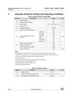
Absolute maximum ratings and operating conditions Table 2: Absolute maximum ratings (AMR)
Open the catalog to page 4
Table 4: Electrical characteristics at VCC+ = 4.5 V with VCC- = 0 V, Vicm = VCC/2, Tamb = 25 °C, and RL = 10 kQ connected to VCC/2 (unless otherwise specified)
Open the catalog to page 5
Notes: Typical value is based on the Vio drift observed after 1000 h at 125 °C extrapolated to 25 °C using the Arrhenius law and assuming an activation energy of 0.7 eV. The operational amplifier is aged in follower mode configuration (see Section 5.5: "Long term input offset voltage drift"). (2) When used in comparator mode, with high differential input voltage, during a long period of time with VCC close to 16 V and Vicm>VCC/2, Vio can experience a permanent drift of a few mV drift. This phenomenon is notably worse at low temperatures.
Open the catalog to page 6
Table 5: Electrical characteristics at VCC+ = 10 V with VCC- = 0 V, Vicm = VCC/2, unless otherwise specified)
Open the catalog to page 7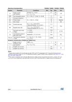
Notes: ( 'Typical value is based on the Vio drift observed after 1000 h at 125 °C extrapolated to 25 °C using the Arrhenius law and assuming an activation energy of 0.7 eV. The operational amplifier is aged in follower mode configuration (see Section 5.5: "Long term input offset voltage drift"). (2) When used in comparator mode, with high differential input voltage, during a long period of time with VCC close to 16 V and Vicm>VCC/2, Vio can experience a permanent drift of a few mV drift. This phenomenon is notably worse at low temperatures.
Open the catalog to page 8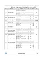
Table 6: Electrical characteristics at VCC+ = 16 V with VCC- = 0 V, Vicm = VCC/2, unless otherwise specified)
Open the catalog to page 9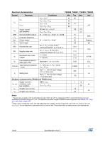
Notes: ( 'Typical value is based on the Vio drift observed after 1000 h at 125 °C extrapolated to 25 °C using the Arrhenius law and assuming an activation energy of 0.7 eV. The operational amplifier is aged in follower mode configuration (see Section 5.5: "Long term input offset voltage drift"). (2) When used in comparator mode, with high differential input voltage, during a long period of time with VCC close to 16 V and Vicm>VCC/2, Vio can experience a permanent drift of a few mV drift. This phenomenon is notably worse at low temperatures.
Open the catalog to page 10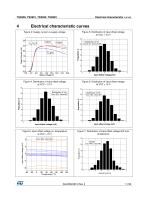
Figure 3: Distribution of input offset voltage at VCC = 4.5 V -2-10 1 2 Input Offset Voltage(mV) Figure 6: Input offset voltage vs. temperature at VCC = 16 V
Open the catalog to page 11
Figure 15: Bode diagram vs. temperature for VCC = 4 V Figure 19: Bode diagram at VCC = 16 V with high common-mode voltage 250 200 150 100 50 C
Open the catalog to page 13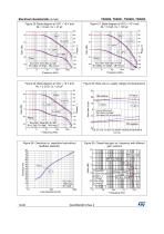
Electrical characteristic curves Figure 20: Bode diagram at VCC = 16 V and RL = 10 kΩ, CL = 47 pF Figure 21: Bode diagram at VCC = 16 V and RL = 10 kΩ, CL = 120 pF Figure 22: Bode diagram at VCC = 16 V and RL = 2.2 kΩ, CL = 20 pF Figure 23: Slew rate vs. supply voltage and temperature Figure 24: Overshoot vs. capacitive load without feedback capacitor Figure 25: Closed loop gain vs. frequency with different gain resistors
Open the catalog to page 14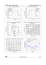
Electrical characteristic curves Figure 26: Large step response Figure 27: Small step response Figure 28: Small step response with feedback capacitor CF Figure 29: Output impedance vs. frequency in closed loop configuration Figure 30: Noise vs. frequency with 16 V supply voltage
Open the catalog to page 15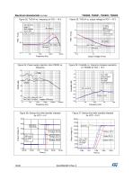
Figure 36: Startup time after standby released for VCC = 4 V Figure 37: Startup time after standby released for VCC = 16 V 20.00 17.50 15.00
Open the catalog to page 16
Application information Application information Operating voltages The TSX92x operational amplifiers can operate from 4 V to 16 V. The parameters are fully specified at 4.5 V, 10 V, and 16 V power supplies. However, parameters are very stable in the full VCC range. Additionally, main specifications are guaranteed in the extended temperature range from -40 to 125 °C. Rail-to-rail input The TSX92x series is designed with two complementary PMOS and NMOS input differential pairs. The device has a rail-to-rail input and the input common mode range is extended from (VCC-) - 0.1 V to (VCC+) + 0.1 V....
Open the catalog to page 17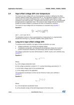
Input offset voltage drift over temperature The maximum input voltage drift over the temperature variation is defined as the offset variation related to offset value measured at 25 °C. The operational amplifier is one of the main circuits of the signal conditioning chain, and the amplifier input offset is a major contributor to the chain accuracy. The signal chain accuracy at 25 °C can be compensated during production at application level. The maximum input voltage drift over temperature enables the system designer to anticipate the effect of temperature variations. The maximum input voltage...
Open the catalog to page 18All STMicroelectronics catalogs and technical brochures
 STGW30NC60KD
14 Pages
 STGB14NC60K STGD14NC60K
16 Pages
 HD1750FX
8 Pages
 TDA75610SLV
42 Pages
 TDA7391
13 Pages
 TDA7376B
15 Pages
 TDA7375V
15 Pages
 TDA2005
25 Pages
 L4989D, L4989MD
19 Pages
 L4938ED L4938EPD
20 Pages
 L4949ED-E L4949EP-E
19 Pages
 L4925
L492514 Pages
 FDA903U
80 Pages
 FDA803U
76 Pages
 FDA903D
82 Pages
 FDA803D
78 Pages
 BALF-SPI2-02D3
13 Pages
 LIS2DTW12
65 Pages
 VL53L0X
40 Pages
 LPS22HH
59 Pages
 Standard products offer overview
13 Pages
 M40SZ100W
20 Pages
 A1C15S12M3
17 Pages
 TS1851
24 Pages
 LMV321
17 Pages
 Serial real-time clock (RTC) ICs
16 Pages
 TDA2003LG
8 Pages
 HCF4541 Programmable Timer
10 Pages
 STA8058 GPS multi-chip module
14 Pages
 TDA7410ND Signal Processor
34 Pages
 TDA7410ND Signal Processor
34 Pages
 TSA1204 DUAL CHANNEL
31 Pages


Archived catalogs
 NEATSwitch
6 Pages
 Power MOSFETs for metering
2 Pages


- Single-pole switch
- Acceleration sensor
- Pressure probe
- Technology switch
- Signal amplifying integrated circuit
- Multipole switch
- Piezoelectric accelerometer
- Transceiver module
- Electronic filter
- Electromechanical switch
- Membrane pressure sensor
- Analog pressure sensor
- Rotary electric switch
- Triaxial acceleration sensor
- Power amplifying integrated circuit
- Distance sensor
- Diode
- STMicroelectronics transistor
- Low-pass electronic filter
- Absolute pressure sensor