- Catalogs
- STMicroelectronics
- TSX712 Low-power, precision, rail-to-rail, 2.7 MHz, 16 V operational amplifier
TSX712 Low-power, precision, rail-to-rail, 2.7 MHz, 16 V operational amplifier
1 /27Pages

TSX712 Low-power, precision, rail-to-rail, 2.7 MHz, 16 V operational amplifier
1 /27Pages
Catalog excerpts
TSX712 Low-power, precision, rail-to-rail, 2.7 MHz, 16 V operational amplifier Datasheet - production data Battery-powered instrumentation Instrumentation amplifier Active filtering DAC buffer High-impedance sensor interface Current sensing (high and low side) Description Features • • • • • • • • • • Low input offset voltage: 200 µV max. Rail-to-rail input and output Low current consumption: 800 µA max. Gain bandwidth product: 2.7 MHz Low supply voltage: 2.7 - 16 V Unity gain stable Low input bias current: 50 pA max. High ESD tolerance: 4 kV HBM Extended temp. range: -40 °C to +125 °C Automotive qualification Related products • • • • • See the TSX711 for single op amp See the TSX7192 for higher speeds with similar precision See the TSX562 for low-power features See the TSX632 for micro-power features See the TSX922 for higher speeds The TSX712 dual, operational amplifier (op amp) offers high precision functioning with low input offset voltage down to a maximum of 200 µV at 25 °C. In addition, its rail-to-rail input and output functionality allows this product to be used on full range input and output without limitation. This is particularly useful for a low-voltage supply such as 2.7 V that the TSX712 is able to operate with. Thus, the TSX712 has the great advantage of offering a large span of supply voltages, ranging from 2.7 V to 16 V. It can be used in multiple applications with a unique reference. Low input bias current performance makes the TSX712 perfect when used for signal conditioning in sensor interface applications. In addition, low-side and high-side current measurements can be easily made thanks to railto-rail functionality. High ESD tolerance (4 kV HBM) and a wide temperature range are also good arguments to use the TSX712 in the automotive market segment. This is information on a product in full production.
Open the catalog to page 1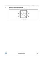
Package pin connections Figure 1: Pin connections (top view)
Open the catalog to page 3
Absolute maximum ratings and operating conditions Absolute maximum ratings and operating conditions Table 1: Absolute maximum ratings (AMR) Symbol VCC Input voltage Input current Storage temperature Thermal resistance junction to ambient (MiniSO8) Thermal resistance junction to ambient (SO8) Maximum junction temperature HBM: human body model ESD Differential input voltage Supply voltage CDM: charged device model Latch-up immunity All voltage values, except the differential voltage are with respect to the network ground terminal. Differential voltages are the non-inverting input terminal with...
Open the catalog to page 4
Electrical characteristics Electrical characteristics Table 3: Electrical characteristics at VCC+ = +4 V with VCC- = 0 V, Vicm = VCC/2, Tamb = 25 ° C, and RL > 10 kΩ connected to VCC/2 (unless otherwise specified) Input offset voltage Input offset voltage drift Input bias current Input offset current Input capacitance Tmin < Top < Tmax Vicm = -0.1 to 2 V, Vout = VCC/2 High level output voltage (voltage drop from VCC+) Supply current per amplifier Tmin < Top < Tmax Isink RL= 2 kΩ tο VCC/2 Low level output voltage Large signal voltage gain Common mode rejection ratio 20 log (ΔVic/ΔVio) Vicm = -0.1...
Open the catalog to page 5
Electrical characteristics Symbol Gain bandwidth product Phase margin Gain margin Positive slew rate Negative slew rate Equivalent input noise voltage Total harmonic distortion + noise Maximum values are guaranteed by design. Typical value is based on the Vio drift observed after 1000h at 125 °C extrapolated to 25 °C using the Arrhenius law and assuming an activation energy of 0.7 eV. The operational amplifier is aged in follower mode configuration (see Section 4.6). Table 4: Electrical characteristics at VCC+ = +10 V with VCC- = 0 V, Vicm = VCC/2, Tamb = 25 °C, and RL > 10 kΩ connected to VCC/2...
Open the catalog to page 6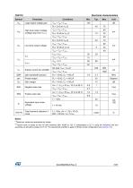
Electrical characteristics Parameter Large signal voltage gain Conditions Tmin < Top < Tmax High level output voltage (voltage drop from VCC+) Low level output voltage Supply current per amplifier Gain margin Positive slew rate Phase margin Negative slew rate Gain bandwidth product Tmin < Top < Tmax Isink Equivalent input noise voltage Total harmonic distortion + noise Maximum values are guaranteed by design. Typical value is based on the Vio drift observed after 1000h at 125 °C extrapolated to 25 °C using the Arrhenius law and assuming an activation energy of 0.7 eV. The operational amplifier...
Open the catalog to page 7
Electrical characteristics Table 5: Electrical characteristics at VCC+ = +16 V with VCC- = 0 V, Vicm = VCC/2, Tamb = 25 °C, and RL > 10 kΩ connected to VCC/2 (unless otherwise specified) Symbol Input offset voltage Input offset voltage drift Input bias current Input offset current Input capacitance Supply voltage rejection ratio 20 log (ΔVcc/ΔVio) Large signal voltage gain Tmin < Top < Tmax Vicm = -0.1 to 14 V, Vout = VCC/2 High level output voltage (voltage drop from VCC+) Supply current per amplifier Tmin < Top < Tmax Isink RL= 2 kΩ Low level output voltage Common mode rejection ratio 20 log...
Open the catalog to page 8
Electrical characteristics Parameter Gain bandwidth product Phase margin Gain margin Negative slew rate Positive slew rate Av = 1, Vout = 10 VPP, 10 % to 90 % Tmin < Top < Tmax Equivalent input noise voltage Total harmonic distortion + Noise Maximum values are guaranteed by design. Typical value is based on the Vio drift observed after 1000h at 125 °C extrapolated to 25 °C using the Arrhenius law and assuming an activation energy of 0.7 eV. The operational amplifier is aged in follower mode configuration (see Section 4.6).
Open the catalog to page 9
Electrical characteristics Figure 2: Supply current vs. supply voltage Figure 3: Input offset voltage distribution at VCC = 16 V 20 Input offset voltage (µV) Input offset voltage (µV) Figure 6: Input offset voltage drift population Figure 7: Input offset voltage vs. supply voltage at VICM = 0 V Input Offset Voltage (µV) Figure 5: Input offset voltage vs. temperature at VCC = 16 V Input offset voltage (µV) Figure 4: Input offset voltage distribution at VCC = 4 V ∆Vio/∆T (µV/ºC)
Open the catalog to page 10All STMicroelectronics catalogs and technical brochures
 STGW30NC60KD
14 Pages
 STGB14NC60K STGD14NC60K
16 Pages
 HD1750FX
8 Pages
 TDA75610SLV
42 Pages
 TDA7391
13 Pages
 TDA7376B
15 Pages
 TDA7375V
15 Pages
 TDA2005
25 Pages
 L4989D, L4989MD
19 Pages
 L4938ED L4938EPD
20 Pages
 L4949ED-E L4949EP-E
19 Pages
 L4925
L492514 Pages
 FDA903U
80 Pages
 FDA803U
76 Pages
 FDA903D
82 Pages
 FDA803D
78 Pages
 BALF-SPI2-02D3
13 Pages
 LIS2DTW12
65 Pages
 VL53L0X
40 Pages
 LPS22HH
59 Pages
 Standard products offer overview
13 Pages
 M40SZ100W
20 Pages
 A1C15S12M3
17 Pages
 TSX923
32 Pages
 TS1851
24 Pages
 LMV321
17 Pages
 Serial real-time clock (RTC) ICs
16 Pages
 TDA2003LG
8 Pages
 HCF4541 Programmable Timer
10 Pages
 STA8058 GPS multi-chip module
14 Pages
 TDA7410ND Signal Processor
34 Pages
 TDA7410ND Signal Processor
34 Pages
 TSA1204 DUAL CHANNEL
31 Pages


Archived catalogs
 NEATSwitch
6 Pages
 Power MOSFETs for metering
2 Pages


- Bourn And Koch single-pole switch
- Bourn And Koch accelerometer
- Bourn And Koch pressure sensor
- Technology switch
- Bourn And Koch signal amplifier
- Multipole switch
- Piezoelectric accelerometer
- Bourn And Koch transceiver
- Bourn And Koch electronic filter
- Electromechanical switch
- Bourn And Koch membrane pressure sensor
- Bourn And Koch analog pressure sensor
- Rotary electric switch
- Triaxial acceleration sensor
- Bourn And Koch power amplifier
- Distance sensor
- Diode
- Bourn And Koch transistor
- Low-pass electronic filter
- Absolute pressure sensor