- Catalogs
- STMicroelectronics
- TSV630, TSV630A, TSV631, TSV631A Rail-to-rail input/output, 60 ?A, 880 kHz, 5 V CMOS operational amplifiers
TSV630, TSV630A, TSV631, TSV631A Rail-to-rail input/output, 60 ?A, 880 kHz, 5 V CMOS operational amplifiers
1 /26Pages

TSV630, TSV630A, TSV631, TSV631A Rail-to-rail input/output, 60 ?A, 880 kHz, 5 V CMOS operational amplifiers
1 /26Pages
Catalog excerpts
TSV630, TSV630A, TSV631, TSV631A Rail-to-rail input/output, 60 μA, 880 kHz, 5 V CMOS operational amplifiers Datasheet - production data Related products • See the TSV52x series for higher merit factor (1.15 MHz for 45 µA) • See the TSV61x (120 kHz for 9 µA) or the TSV62x (420 kHz for 29 µA) for more power savings Applications • Battery-powered applications • Portable devices • Active filtering • Medical instrumentation Description The TSV630 and TSV631 devices are single operational amplifiers offering low voltage, low power operation, and rail-to-rail input and output. Features • Low offset voltage: 500 µV max (A version) • Low power consumption: 60 µA typ at 5 V • Low supply voltage: 1.5 V - 5.5 V • Gain bandwidth product: 880 kHz typ • Unity gain stability • Low power shutdown mode: 5 nA typ • High output current: 63 mA at VCC = 5 V • Low input bias current: 1 pA typ • Rail-to-rail input and output • Extended temperature range: -40 °C to 125 °C • Automotive qualification October 2013 This is information on a product in full production. These devices have a very low input bias current and a low offset voltage making them ideal for applications that require precision. They can operate at power supplies ranging from 1.5 V to 5.5 V, and are therefore very suitable for batterypowered devices, extending battery life. These op-amps feature an excellent speed/power consumption ratio, offering an 880 kHz gain bandwidth while consuming only 60 µA at a 5 V supply voltage. They are unity gain stable for capacitive loads up to 100 pF. The devices are internally adjusted to provide very narrow dispersion of AC and DC parameters. The TSV630 provides a shutdown function. All devices are offered in micropackages and are guaranteed for industrial temperature ranges from -40° C to +125° C. These features combined make the TSV630 and TSV631 ideal for sensor interfaces, batterysupplied and portable applications, as well as active filtering.
Open the catalog to page 1
Absolute maximum ratings and operating conditions . . . . . . . . . . . . . 4 Driving resistive and capacitive loads . . . . . . . . . . . . . . . . . . . . . . . . . . . 15 DFN6 1.2x1.3 package mechanical data . . . . . . . . . . . . . . . . . . . . . . . . . 18 SC70-6 (or SOT323-6) package mechanical data . . . . . . . . . . . . . . . . . . 20 SOT23-6 package mechanical data . . . . . . . . . . . . . . . . . . . . . . . . . . . . . 22 SC70-5 (or SOT323-5) package mechanical data . . . . . . . . . . . . . . . . . . 23 SOT23-5 package mechanical data . . . . . . . . . . . . . . . . . . . . ....
Open the catalog to page 2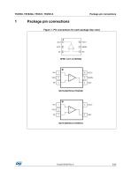
Figure 1. Pin connections for each package (top view)
Open the catalog to page 3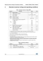
Absolute maximum ratings and operating conditions Absolute maximum ratings and operating conditions Table 1. Absolute maximum ratings (AMR) Symbol VCC Vid Vin Iin SHDN Parameter Supply voltage Input current Shutdown voltage Differential input voltage Input voltage Storage temperature Maximum junction temperature Latchup immunity 1. All voltage values, except the differential voltage, is with respect to network ground terminal. 2. The differential voltage is the non-inverting input terminal with respect to the inverting input terminal. 3. VCC-Vin must not exceed 6 V. 4. Input current must be limited...
Open the catalog to page 4
Electrical characteristics Electrical characteristics Table 3. Electrical characteristics at VCC+ = +1.8 V with VCC- = 0 V, Vicm = VCC/2, Tamb = 25 ° C and RL connected to VCC/2 (unless otherwise specified) Symbol Offset voltage Input offset current (Vout = VCC/2) Input bias current (Vout = VCC/2) Common mode rejection ratio 20 log (ΔVic/ΔVio) Large signal voltage gain High level output voltage Low level output voltage Isink Iout Isource ICC Input offset voltage drift Supply current SHDN = VCC+ Gain bandwidth product Phase margin Gain margin Slew rate Equivalent input noise voltage
Open the catalog to page 5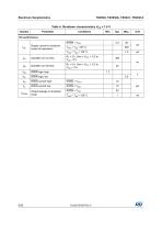
Electrical characteristics TSV630, TSV630A, TSV631, TSV631A Table 4. Shutdown characteristics VCC = 1.8 V Supply current in shutdown mode (all operators) Amplifier turn-on time Amplifier turn-off time SHDN logic high SHDN current high Output leakage in shutdown mode
Open the catalog to page 6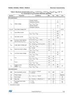
Electrical characteristics Table 5. Electrical characteristics at VCC+ = +3.3 V, VCC- = 0 V, Vicm = VCC/2, Tamb = 25 ° C, RL connected to VCC/2 (unless otherwise specified) Symbol Offset voltage Input offset current Input bias current Common mode rejection ratio 20 log (ΔVic/ΔVio) Large signal voltage gain High level output voltage Low level output voltage Isink Iout Isource ICC Input offset voltage drift Supply current SHDN = VCC+ Gain bandwidth product Phase margin Gain margin Slew rate Equivalent input noise voltage
Open the catalog to page 7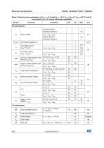
Electrical characteristics Table 6. Electrical characteristics at VCC+ = +5 V with VCC- = 0 V, Vicm = VCC/2, Tamb = 25° C and RL connected to VCC/2 (unless otherwise specified) Symbol Offset voltage Input offset voltage drift Input offset current (Vout = VCC/2) Input bias current (Vout = VCC/2) Common mode rejection ratio 20 log (ΔVic/ΔVio) Supply voltage rejection ratio 20 log (ΔVCC/ΔVio) Large signal voltage gain High level output voltage Low level output voltage Isink Iout Isource ICC Supply current SHDN = VCC+ Tmin < Top < Tmax Tmin < Top < Tmax 0 V to 5 V, Vout = 2.5 V Gain bandwidth product...
Open the catalog to page 8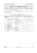
Electrical characteristics Table 6. Electrical characteristics at VCC+ = +5 V with VCC- = 0 V, Vicm = VCC/2, Tamb = 25° C and RL connected to VCC/2 (unless otherwise specified) (continued) Symbol Equivalent input noise voltage Total harmonic distortion Table 7. Shutdown characteristics VCC = 5 V Symbol Supply current in shutdown mode (all operators) Amplifier turn-on time Amplifier turn-off time SHDN logic high SHDN current high Output leakage in shutdown mode
Open the catalog to page 9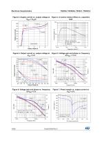
Electrical characteristics Figure 2. Supply current vs. supply voltage at Figure 3. In-series resistor (Riso) vs. capacitive Follower configuration Figure 4. Output current vs. output voltage at Figure 5. Voltage gain and phase vs. frequency
Open the catalog to page 10All STMicroelectronics catalogs and technical brochures
 STGW30NC60KD
14 Pages
 STGB14NC60K STGD14NC60K
16 Pages
 HD1750FX
8 Pages
 TDA75610SLV
42 Pages
 TDA7391
13 Pages
 TDA7376B
15 Pages
 TDA7375V
15 Pages
 TDA2005
25 Pages
 L4989D, L4989MD
19 Pages
 L4938ED L4938EPD
20 Pages
 L4949ED-E L4949EP-E
19 Pages
 L4925
L492514 Pages
 FDA903U
80 Pages
 FDA803U
76 Pages
 FDA903D
82 Pages
 FDA803D
78 Pages
 BALF-SPI2-02D3
13 Pages
 LIS2DTW12
65 Pages
 VL53L0X
40 Pages
 LPS22HH
59 Pages
 Standard products offer overview
13 Pages
 M40SZ100W
20 Pages
 A1C15S12M3
17 Pages
 TSX923
32 Pages
 TS1851
24 Pages
 LMV321
17 Pages
 Serial real-time clock (RTC) ICs
16 Pages
 TDA2003LG
8 Pages
 HCF4541 Programmable Timer
10 Pages
 STA8058 GPS multi-chip module
14 Pages
 TDA7410ND Signal Processor
34 Pages
 TDA7410ND Signal Processor
34 Pages
 TSA1204 DUAL CHANNEL
31 Pages


Archived catalogs
 NEATSwitch
6 Pages
 Power MOSFETs for metering
2 Pages


- Single-pole switch
- Acceleration sensor
- Pressure probe
- Technology switch
- Signal amplifying integrated circuit
- Multipole switch
- Piezoelectric accelerometer
- Transceiver module
- Electronic filter
- Electromechanical switch
- Analog pressure sensor
- Membrane pressure sensor
- Rotary electric switch
- Triaxial acceleration sensor
- Power amplifying integrated circuit
- Distance sensor
- Diode
- STMicroelectronics transistor
- Low-pass electronic filter
- Absolute pressure sensor