- Catalogs
- STMicroelectronics
- TS391 Low power, single voltage comparator
TS391 Low power, single voltage comparator
1 /12Pages

TS391 Low power, single voltage comparator
1 /12Pages
Catalog excerpts

Low-power single voltage comparator Datasheet — production data ■ Wide single supply voltage range or dual ■ Very low supply current (0.2 mA) independent of supply voltage (1 mW/comparator at +5 V) ■ Low input bias current: 25 nA typ. ■ Low input offset current: +5 nA typ. ■ Low input offset voltage: +1 mV typ. ■ Input common-mode voltage range includes ■ Low output saturation voltage: 250 mV typ. ■ Differential input voltage range equal to the supply voltage ■ TTL, DTL, ECL, CMOS compatible outputs This device consists of a low-power voltage comparator designed specifically to operate from a single supply over a wide range of voltages. Operation from split power supplies is also This comparator also has a unique characteristic in that the input common-mode voltage range includes ground, even though operated from a single power supply voltage. (Plastic package) (Plastic micropackage) This is information on a product in full production. www.sf.com
Open the catalog to page 1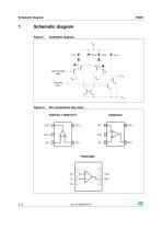
Schematic diagram Schematic diagram Figure 1. Inverting input
Open the catalog to page 2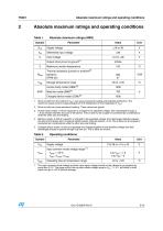
Absolute maximum ratings and operating conditions Absolute maximum ratings and operating conditions Table 1. Absolute maximum ratings (AMR) Differential input voltage Input voltage Supply voltage Maximum junction temperature Thermal resistance junction to SOT23-5 DFN8 2x2 Storage temperature range Human body model (HBM)(3) Charged device model 1. Short-circuits from the output to VCC+ can cause excessive heating and potential destruction. The maximum output current is approximately 20 mA independent of the magnitude of VCC+. 2. Short-circuits can cause excessive heating. These values are typical....
Open the catalog to page 3
Electrical characteristics Electrical characteristics VCC+ = +5 V, VCC- = 0 V, Tamb = 25°C (unless otherwise specified) Input offset voltage (1) Input offset current Input bias current (2) Test conditions Tmin ≤ Tamb ≤ Tmax Tmin ≤ Tamb ≤ Tmax Tmin ≤ Tamb ≤ Tmax Large signal voltage gain Supply current VCC+ = 5V, no load VCC+ = 30V, no load Differential input voltage (3) Output sink current Low level output voltage High level output current Small signal response time Large signal response time 1. At output switch point, VO ≈ 1.4V, RS = 0Ω with VCC+ from 5V to 30V and over the full input common-mode...
Open the catalog to page 4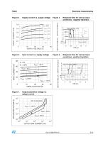
Electrical characteristics Supply current vs. supply voltage Figure 6. OUTPUT VOLTAGE (V) Input current vs. supply voltage Response time for various input overdrives - negative transition Response time for various input overdrives - positive transition Output saturation voltage vs. output current OUTPUT SINK CURRENT (mA)
Open the catalog to page 5
Package information Package information In order to meet environmental requirements, ST offers these devices in different grades of ECOPACK® packages, depending on their level of environmental compliance. ECOPACK® specifications, grade definitions and product status are available at: www.st.com. ECOPACK® is an ST trademark.
Open the catalog to page 6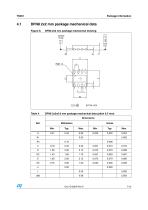
Package information 4.1 DFN8 2x2 mm package mechanical data Figure 8. DFN8 2x2 mm package mechanical drawing
Open the catalog to page 7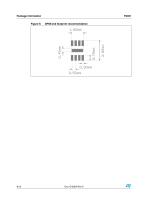
Package information Figure 9. DFN8 2x2 footprint recommendation
Open the catalog to page 8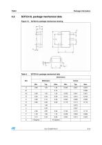
Package information SOT23-5L package mechanical data Figure 10. SOT23-5L package mechanical drawing SOT23-5L package mechanical data Dimensions
Open the catalog to page 9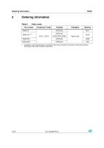
Ordering information Ordering information Table 6. Order codes Part number Temperature range Tape & reel 1. Qualification and characterization according to AEC Q100 and Q003 or equivalent, advanced screening according to AEC Q001 & Q002 or equivalent.
Open the catalog to page 10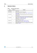
Revision history Revision history Table 7. Document revision history Initial release. PPAP reference inserted in the document. Added values for Rthja, Rthjc and ESD in Table 1: Absolute maximum ratings (AMR). Added footnote for automotive grade order code in order codes table. Updated format. Corrected ESD tolerance values for human body model and machine model in Table 1: Absolute maximum ratings (AMR) and added ESD tolerance value for charged device model. Updated note 1 in Table 6: Order codes. Added TS391R pinout on page 1. Modified VCC range in Table 2: Operating conditions. Added TS391RILT...
Open the catalog to page 11
Please Read Carefully: Information in this document is provided solely in connection with ST products. STMicroelectronics NV and its subsidiaries (“ST”) reserve the right to make changes, corrections, modifications or improvements, to this document, and the products and services described herein at any time, without notice. All ST products are sold pursuant to ST’s terms and conditions of sale. Purchasers are solely responsible for the choice, selection and use of the ST products and services described herein, and ST assumes no liability whatsoever relating to the choice, selection or use of...
Open the catalog to page 12All STMicroelectronics catalogs and technical brochures
 STGW30NC60KD
14 Pages
 STGB14NC60K STGD14NC60K
16 Pages
 HD1750FX
8 Pages
 TDA75610SLV
42 Pages
 TDA7391
13 Pages
 TDA7376B
15 Pages
 TDA7375V
15 Pages
 TDA2005
25 Pages
 L4989D, L4989MD
19 Pages
 L4938ED L4938EPD
20 Pages
 L4949ED-E L4949EP-E
19 Pages
 L4925
L492514 Pages
 FDA903U
80 Pages
 FDA803U
76 Pages
 FDA903D
82 Pages
 FDA803D
78 Pages
 BALF-SPI2-02D3
13 Pages
 LIS2DTW12
65 Pages
 VL53L0X
40 Pages
 LPS22HH
59 Pages
 Standard products offer overview
13 Pages
 M40SZ100W
20 Pages
 A1C15S12M3
17 Pages
 TSX923
32 Pages
 TS1851
24 Pages
 LMV321
17 Pages
 Serial real-time clock (RTC) ICs
16 Pages
 TDA2003LG
8 Pages
 HCF4541 Programmable Timer
10 Pages
 STA8058 GPS multi-chip module
14 Pages
 TDA7410ND Signal Processor
34 Pages
 TDA7410ND Signal Processor
34 Pages
 TSA1204 DUAL CHANNEL
31 Pages


Archived catalogs
 NEATSwitch
6 Pages
 Power MOSFETs for metering
2 Pages


- Single-pole switch
- Acceleration sensor
- Pressure probe
- Technology switch
- Signal amplifying integrated circuit
- Multipole switch
- Piezoelectric accelerometer
- Transceiver module
- Electronic filter
- Electromechanical switch
- Analog pressure sensor
- Membrane pressure sensor
- Rotary electric switch
- Triaxial acceleration sensor
- Power amplifying integrated circuit
- Distance sensor
- Diode
- STMicroelectronics transistor
- Low-pass electronic filter
- Absolute pressure sensor