TS1851
1 /24Pages

TS1851
1 /24Pages
Catalog excerpts

Features ■ Operating range from Vcc = 1.8 to 6 V ■ Rail-to-rail input and output ■ Extended V^ (Vcc- - 0.2 V to Vcc + + 0.2 V) ■ Low supply current (120 pA) ■ Good accuracy (1 mV max for A version) ■ Gain bandwidth product (530 kHz) ■ High unity gain stability (able to drive 500 pF) ■ ESD tolerance (2 kV) ■ Latch-up immunity ■ Available in SOT23-5 micropackage Applications ■ Two-cell battery-powered systems ■ Battery-powered electronic equipment ■ cordless phones ■ cellular phones ■ Laptops ■ PDAs Description The TS185x (single, dual and quad) can operate with voltages as low as 1.8 V. They feature both input and output rail-to-rail (1.71 at Vcc = 1.8 V, Rl = 2 kQ), 120 pA current consumption and 530 kHz gain bandwidth product. With this low consumption and a sufficient GBP for many applications, these operational amplifiers are well-suited to all kinds of battery supplied and portable applications. The TS1851 is housed in the space-saving 5-pin SOT23-5 package, which simplifies board design (outside dimensions are 2.8 mm x 2.9 mm). Table 1. Device summary
Open the catalog to page 1
Absolute maximum ratings and operating conditions . . . . . . . . . . . . . 3
Open the catalog to page 2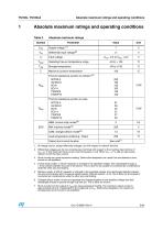
TS185x, TS185xA Absolute maximum ratings and operating conditions Table 2. Absolute maximum ratings 1. All voltage values, except differential voltages, are with respect to network terminal. 2. Differential voltages are the non-inverting input terminal with respect to the inverting input terminal. If Vid > ±1 V, the maximum input current must not exceed ±1 mA. When Vjd > ±1 V, add an input series resistor to limit the input current. 3. Short-circuits can cause excessive heating. Destructive dissipation can result from simultaneous short-circuits on all amplifiers. 4. Human body model: a 100 pF...
Open the catalog to page 3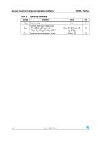
Absolute maximum ratings and operating conditions TS185x, TS185xA Table 3. Operating conditions
Open the catalog to page 4
Table 4. Electrical characteristics measured at Vcc+ = +1.8 V, Vcc. = 0 V, with CL and RL connected to Vcc/2, Tamb = 25°C (unless otherwise specified) (1) 1. All parameter limits at temperatures other than 25°C are guaranteed by correlation. 2. Maximum values include unavoidable inaccuracies of the industrial tests.
Open the catalog to page 5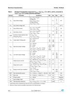
Table 5. Electrical characteristics measured at Vcc+ = +3 V, Vcc_ = 0 V, with CL and RL connected to Vcc/2, Tamb = 25°C (unless otherwise specified) (1) 1. All parameter limits at temperatures other than 25°C are guaranteed by correlation. 2. Maximum values include unavoidable inaccuracies of the industrial tests.
Open the catalog to page 6
Table 6. Electrical characteristics measured at Vcc+ = +5 V, Vcc_ = 0 V, with CL and RL connected to Vcc/2, Tamb = 25°C (unless otherwise specified) (1) 1. All parameter limits at temperatures other than 25°C are guaranteed by correlation. 2. Maximum values include unavoidable inaccuracies of the industrial tests.
Open the catalog to page 7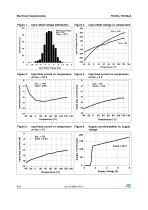
Electrical characteristics Input offset voltage distribution Input Voltage Drift (µV) 400 488 pieces tested Vcc = 10V Temp = +25°C Input offset voltage vs. temperature Vcc = 1.8V Input Offset Voltage (mV) Input bias current vs. temperature at Vcc = 1.8 V Input bias current (nA) Input bias current (nA) Input bias current vs. temperature at Vcc = 5 V Supply current/amplifier vs. supply voltage Input bias current (nA) Input bias current vs. temperature at Vcc = 3 V
Open the catalog to page 8
Supply current/amplifier vs. temperature Common Mode Rejection (dB) Electrical characteristics Common mode rejection vs. temperaturej at Vcc = 1.8 p V Common mode rejection vs. temperaturej at Vcc = 3 Vp Figure 10. Common mode rejection vs. temperature at Vcc = 5 V Common Mode Rejection (dB) Common Mode Rejection (dB) Supply Voltage Rejection (dB) Supply Voltage Rejection (dB) Figure 12. Supply voltage rejection vs. temperature at Vcc = 3 V Figure 11. Supply voltage rejection vs. temperature at Vcc = 2 V
Open the catalog to page 9
Electrical characteristics Figure 13. Supply voltage rejection vs. temperature at Vcc = 5 V Figure 14. Open loop gain vs. temperature at Vcc = 1.8 V 110 Open Loop Gain (dB) Supply Voltage Rejection (dB) Open Loop Gain (dB) Open Loop Gain (dB) Figure 18. Low level output voltage vs. temperature, RL = 10 kΩ Figure 17. High level output voltage vs. temperature, RL = 10 kΩ Figure 16. Open loop gain vs. temperature at Vcc = 5 V Figure 15. Open loop gain vs. temperature at Vcc = 3 V
Open the catalog to page 10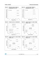
Electrical characteristics Figure 20. Low level output voltage vs. temperature, RL = 2 kΩ Figure 19. High level output voltage vs. temperature, RL = 2 kΩ Vcc = 5V Figure 23. Output current vs. output voltage at Vcc = 3 V Figure 24. Output current vs. output voltage at Vcc = 5 V 80 Figure 22. Output current vs. output voltage at Vcc = 1.8 V Figure 21. Output current vs. temperature
Open the catalog to page 11
Figure 25. Gain and phase vs. frequency at Vcc = 1.8 V Figure 26. Gain and phase vs. frequency at Vcc = 5 V Figure 27. Gain bandwidth product vs. temperature Figure 28. Gain bandwidth product vs. supply voltage
Open the catalog to page 12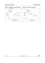
Electrical characteristics Figure 37. Distortion vs. output voltage at Vcc = 5 V Figure 38. Distortion vs. frequency 1.000
Open the catalog to page 14
Package information Package information In order to meet environmental requirements, ST offers these devices in different grades of ECOPACK® packages, depending on their level of environmental compliance. ECOPACK® specifications, grade definitions and product status are available at: www.st.com. ECOPACK® is an ST trademark.
Open the catalog to page 15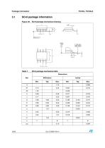
SO-8 package information Figure 39. SO-8 package mechanical drawing
Open the catalog to page 16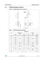
Table 8. TSSOP8 package mechanical data
Open the catalog to page 17
Figure 41. MiniSO-8 package mechanical drawing Table 9. MiniSO-8 package mechanical data
Open the catalog to page 18
Table 10. SO-14 package mechanical data
Open the catalog to page 19
Table 11. TSSOP14 package mechanical data
Open the catalog to page 20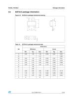
Table 12. SOT23-5L package mechanical data
Open the catalog to page 21
Table 13. Order codes
Open the catalog to page 22
Table 14. Document revision history
Open the catalog to page 23
Please Read Carefully: Information in this document is provided solely in connection with ST products. STMicroelectronics NV and its subsidiaries (“ST”) reserve the right to make changes, corrections, modifications or improvements, to this document, and the products and services described herein at any time, without notice. All ST products are sold pursuant to ST’s terms and conditions of sale. Purchasers are solely responsible for the choice, selection and use of the ST products and services described herein, and ST assumes no liability whatsoever relating to the choice, selection or use of...
Open the catalog to page 24All STMicroelectronics catalogs and technical brochures
 STGW30NC60KD
14 Pages
 STGB14NC60K STGD14NC60K
16 Pages
 HD1750FX
8 Pages
 TDA75610SLV
42 Pages
 TDA7391
13 Pages
 TDA7376B
15 Pages
 TDA7375V
15 Pages
 TDA2005
25 Pages
 L4989D, L4989MD
19 Pages
 L4938ED L4938EPD
20 Pages
 L4949ED-E L4949EP-E
19 Pages
 L4925
L492514 Pages
 FDA903U
80 Pages
 FDA803U
76 Pages
 FDA903D
82 Pages
 FDA803D
78 Pages
 BALF-SPI2-02D3
13 Pages
 LIS2DTW12
65 Pages
 VL53L0X
40 Pages
 LPS22HH
59 Pages
 Standard products offer overview
13 Pages
 M40SZ100W
20 Pages
 A1C15S12M3
17 Pages
 TSX923
32 Pages
 LMV321
17 Pages
 Serial real-time clock (RTC) ICs
16 Pages
 TDA2003LG
8 Pages
 HCF4541 Programmable Timer
10 Pages
 STA8058 GPS multi-chip module
14 Pages
 TDA7410ND Signal Processor
34 Pages
 TDA7410ND Signal Processor
34 Pages
 TSA1204 DUAL CHANNEL
31 Pages


Archived catalogs
 NEATSwitch
6 Pages
 Power MOSFETs for metering
2 Pages


- Single-pole switch
- Acceleration sensor
- Pressure probe
- Technology switch
- Signal amplifying integrated circuit
- Multipole switch
- Piezoelectric accelerometer
- Transceiver module
- Electronic filter
- Electromechanical switch
- Analog pressure sensor
- Membrane pressure sensor
- Rotary electric switch
- Triaxial acceleration sensor
- Power amplifying integrated circuit
- Distance sensor
- Diode
- STMicroelectronics transistor
- Low-pass electronic filter
- Absolute pressure sensor