- Catalogs
- STMicroelectronics
- TDA75610SLV
TDA75610SLV
1 /42Pages

TDA75610SLV
1 /42Pages
Catalog excerpts

TDA75610SLV 4 x 45 W power amplifier with full I2C diagnostics, high efficiency and low voltage operation Datasheet - production data Improved SVR suppression during battery transients Capable to operate down to 6 V (e.g. “Start-stop”) Flexiwatt27 (Horiz.) Description The TDA75610SLV is a new quad bridge car radio amplifier, designed in BCD technology, in order to include a wide range of innovative features in a very compact and flexible device. The TDA75610SLV is equipped with the most complete diagnostics array that communicates the status of each speaker through the I2C bus. Multipower BCD technology MOSFET output power stage DMOS power output High efficiency (class SB) High output power capability 4x25 W/4 Ω @ 14.4 V, 1 kHz, 10% THD, 4 x 45 W max power 2 Ω driving capability (64 W max power) Full I2C bus driving: – Standby – Independent front/rear soft play/mute – Selectable gain 26 dB /16 dB (for low noise line output function) – High efficiency enable/disable – I2C bus digital diagnostics (including DC and AC load detection) Flexible fault detection through integrated diagnostic DC offset detection Four independent short circuit protection Clipping detector pin with selectable threshold (2 %/10 %) The dissipated output power under average listening condition is significantly reduced when compared to the conventional class AB solutions, thanks to the patented 'class SB' efficiency concept. TDA75610SLV has been designed to be very robust against several kinds of misconnections. It is moreover compliant to the most recent OEM specifications for low voltage operation (so called 'start-stop' battery profile during engine stop), helping car manufacturers to reduce the overall emissions and thus contributing to environment protection. The ST BCD in combination with 'class SB' efficiency and 'intelligent power' has been sold in million of units to most known car manufacturers, the TDA75610SLV is the latest and most compact member of this power amplifiers family. Table 1. Device summary Order code Tube Tape and reel Linear thermal shutdown with multiple thermal warning Very robust against misconnections December 2014 This is information on a product in full production.
Open the catalog to page 1
Block diagram and application circuits . . . . . . . . . . . . . . . . . . . . . . . . . 6 Absolute maximum ratings . . . . . . . . . . . . . . . . . . . . . . . . . . . . . . . . . . . . 10 Typical electrical characteristics curves . . . . . . . . . . . . . . . . . . . . . . . . . . 15 Diagnostics functional description . . . . . . . . . . . . . . . . . . . . . . . . . . . . 18 4.1 4.2 Output DC offset detection . . . . . . . . . . . . . . . . . . . . . . . . . . . . . . . . . . . . 21 Battery transitions management . . . . . . . . . . . . . . . . . . . . . . . . . . . . . . 25 7.1 7.2 Low voltage...
Open the catalog to page 2
Start and stop conditions . . . . . . . . . . . . . . . . . . . . . . . . . . . . . . . . . . . . 30 Examples of bytes sequence . . . . . . . . . . . . . . . . . . . . . . . . . . . . . . . . . 36
Open the catalog to page 3
List of tables Table 1. Table 2. Table 3. Table 4. Table 5. Table 6. Table 7. Table 8. Table 9. Table 10. Table 11. Table 12. Table 13. Device summary . . . . . . . . . . . . . . . . . . . . . . . . . . . . . . . . . . . . . . . . . . . . . . . . . . . . . . . . . . 1 Pin list description . . . . . . . . . . . . . . . . . . . . . . . . . . . . . . . . . . . . . . . . . . . . . . . . . . . . . . . . . 9 Absolute maximum ratings . . . . . . . . . . . . . . . . . . . . . . . . . . . . . . . . . . . . . . . . . . . . . . . . . 10 Thermal data. . . . . . . . . . . . . . . . . . . . . . . . . . . ....
Open the catalog to page 4
List of figures Figure 1. Figure 2. Figure 3. Figure 4. Figure 5. Figure 6. Figure 7. Figure 8. Figure 9. Figure 10. Figure 11. Figure 12. Figure 13. Figure 14. Figure 15. Figure 16. Figure 17. Figure 18. Figure 19. Figure 20. Figure 21. Figure 22. Figure 23. Figure 24. Figure 25. Figure 26. Figure 27. Figure 28. Figure 29. Figure 30. Figure 31. Figure 32. Figure 33. Figure 34. Figure 35. Figure 36. Figure 37. Figure 38. Figure 39. Figure 40. Figure 41. Figure 42. Figure 43. Figure 44. Figure 45. Block diagram . . . . . . . . . . . . . . . . . . . . . . . . . . . . . . . . . . . . . . . . . ....
Open the catalog to page 5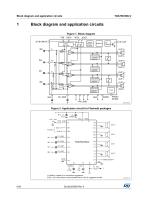
Block diagram and application circuits Block diagram and application circuits Figure 1. Block diagram Figure 2. Application circuit for Flexiwatt packages
Open the catalog to page 6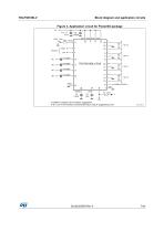
Block diagram and application circuits Figure 3. Application circuit for PowerSO package
Open the catalog to page 7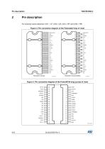
Pin description For channel name reference: CH1 = LF, CH2 = LR, CH3 = RF and CH4 = RR. Figure 4. Pin connection diagram of the Flexiwatt27 (top of view) Figure 5. Pin connection diagram of the PowerSO36 slug up (top of view)
Open the catalog to page 8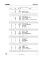
Pin description Table 2. Pin list description I2C bus data pin/gain selector Address selector pin/ I2C bus disable (legacy select) Clip detector output pin Channel 4, + output I2C bus clock/HE selector Channel 4 output power ground Not connected Channel 2 output power ground Channel 2, + output Not connected Channel 1 output power ground Channel 1, + output Not connected AC ground Channel 3, + output Channel 3 output power ground
Open the catalog to page 9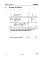
Electrical specifications Electrical specifications Absolute maximum ratings Table 3. Absolute maximum ratings Symbol Operating supply voltage Peak supply voltage (for tmax = 50 ms) Vpeak GNDmax VCK, VDATA Ground pins voltage CK and DATA pin voltage Clip detector voltage IO Ptot Tstg, Tj Tamb Output peak current (not repetitive tmax = 100ms) Output peak current (repetitive f > 10 kHz) Power dissipation Tcase = 70°C Operative temperature range 1. For RL = 2 Ω the output current limit might be reached for VOP > 16 V; thus triggering self-protection. 2. A suitable dissipation system should be used...
Open the catalog to page 10
Electrical specifications Electrical characteristics Refer to the test circuit, VS = 14.4 V; RL = 4 Ω; f = 1 kHz; GV = 26 dB; Tamb = 25 °C; unless otherwise specified. Tested at Tamb = 25 °C and Thot = 105 °C; functionality guaranteed for Tj = -40 °C to 150 °C. Table 5. Electrical characteristics Test condition Supply voltage range Total quiescent drain current Input impedance Min. supply mute threshold Offset voltage Mute & play Dump threshold Standby current Supply voltage rejection Turn on timing (Mute play transition) Turn off timing (Play mute transition) Average junction temperature for...
Open the catalog to page 11All STMicroelectronics catalogs and technical brochures
 STGW30NC60KD
14 Pages
 STGB14NC60K STGD14NC60K
16 Pages
 HD1750FX
8 Pages
 TDA7391
13 Pages
 TDA7376B
15 Pages
 TDA7375V
15 Pages
 TDA2005
25 Pages
 L4989D, L4989MD
19 Pages
 L4938ED L4938EPD
20 Pages
 L4949ED-E L4949EP-E
19 Pages
 L4925
L492514 Pages
 FDA903U
80 Pages
 FDA803U
76 Pages
 FDA903D
82 Pages
 FDA803D
78 Pages
 BALF-SPI2-02D3
13 Pages
 LIS2DTW12
65 Pages
 VL53L0X
40 Pages
 LPS22HH
59 Pages
 Standard products offer overview
13 Pages
 M40SZ100W
20 Pages
 A1C15S12M3
17 Pages
 TSX923
32 Pages
 TS1851
24 Pages
 LMV321
17 Pages
 Serial real-time clock (RTC) ICs
16 Pages
 TDA2003LG
8 Pages
 HCF4541 Programmable Timer
10 Pages
 STA8058 GPS multi-chip module
14 Pages
 TDA7410ND Signal Processor
34 Pages
 TDA7410ND Signal Processor
34 Pages
 TSA1204 DUAL CHANNEL
31 Pages


Archived catalogs
 NEATSwitch
6 Pages
 Power MOSFETs for metering
2 Pages


- Single-pole switch
- Acceleration sensor
- Pressure probe
- Technology switch
- Signal amplifying integrated circuit
- Multipole switch
- Piezoelectric accelerometer
- Transceiver module
- Electronic filter
- Electromechanical switch
- Membrane pressure sensor
- Analog pressure sensor
- Rotary electric switch
- Triaxial acceleration sensor
- Distance sensor
- Diode
- STMicroelectronics transistor
- Low-pass electronic filter
- Absolute pressure sensor