- Catalogs
- STMicroelectronics
- TDA7410ND Signal Processor
TDA7410ND Signal Processor
1 /34Pages

TDA7410ND Signal Processor
1 /34Pages
Catalog excerpts

February 2007 Rev 2 1/34 1 TDA7410ND Signal processor for car radio applications Features ¡ Device Includes Audio Processor, Stereo Decoder And Noiseblanker ¡ No External Components Required ¡ Fully Programmable Via I2C Bus ¡ Softstep Volume and Bass ¡ Low Distortion ¡ Low Noise ¡ SO20 Package Description TDA7410ND is a signal processor specifically designed for car radio applications. The device includes a complete audioprocessor and a stereo decoder with noiseblanker, stereoblend and all signal processing functions for car radio system. Switched-capacitors design technique allows the users to enjoy these features without external components or adjustments. This means higher quality and reliability as well as overall cost saving. The device is fully programmable by I2C bus interface allowing customization of key device parameters, especially filter characteristics.. SO20 Table 1. Device summary Part number Package Packing TDA7410ND SO20 Tube TDA7410NDTR SO20 Tape and reel www.st.com
Open the catalog to page 1
Contents TDA7410ND 2/34 Contents 1 Block diagram . . . . . . . . . . . . . . . . . . . . . . . . . . . . . . . . . . . . . . . . . . . . . . 6 2 Pins description and connection diagram . . . . . . . . . . . . . . . . . . . . . . . 7 2.1 Connection diagram . . . . . . . . . . . . . . . . . . . . . . . . . . . . . . . . . . . . . . . . . . 7 2.2 Pin description . . . . . . . . . . . . . . . . . . . . . . . . . . . . . . . . . . . . . . . . . . . . . . 7 3 Audio Processor Part . . . . . . . . . . . . . . . . . . . . . . . . . . . . . . . . . . . . . . . . 8 4 Electrical Specification . . . . . ....
Open the catalog to page 2
TDA7410ND Contents 3/34 6.8 Highcut Control . . . . . . . . . . . . . . . . . . . . . . . . . . . . . . . . . . . . . . . . . . . . . 21 7 Functional description of the noiseblanker . . . . . . . . . . . . . . . . . . . . . 22 7.1 Trigger path . . . . . . . . . . . . . . . . . . . . . . . . . . . . . . . . . . . . . . . . . . . . . . . 22 7.2 Automatic noise controlled threshold adjustment (ATC) . . . . . . . . . . . . . . 22 7.3 Automatic threshold control . . . . . . . . . . . . . . . . . . . . . . . . . . . . . . . . . . . 23 7.4 Over deviation detector . . . . . . . . . . . . . . . . . ....
Open the catalog to page 3
List of tables TDA7410ND 4/34 List of tables Table 1. Device summary . . . . . . . . . . . . . . . . . . . . . . . . . . . . . . . . . . . . . . . . . . . . . . . . . . . . . . . . . . 1 Table 2. Pins list . . . . . . . . . . . . . . . . . . . . . . . . . . . . . . . . . . . . . . . . . . . . . . . . . . . . . . . . . . . . . . . . . 7 Table 3. Absolute maximum ratings . . . . . . . . . . . . . . . . . . . . . . . . . . . . . . . . . . . . . . . . . . . . . . . . . . 9 Table 4. Supply. . . . . . . . . . . . . . . . . . . . . . . . . . . . . . . . . . . . . . . . . . . . . . . . . . . . . . ....
Open the catalog to page 4
TDA7410ND List of figures 5/34 List of figures Figure 1. Block diagram. . . . . . . . . . . . . . . . . . . . . . . . . . . . . . . . . . . . . . . . . . . . . . . . . . . . . . . . . . . . 6 Figure 2. Connection diagram . . . . . . . . . . . . . . . . . . . . . . . . . . . . . . . . . . . . . . . . . . . . . . . . . . . . . . . 7 Figure 3. Input Stage . . . . . . . . . . . . . . . . . . . . . . . . . . . . . . . . . . . . . . . . . . . . . . . . . . . . . . . . . . . . . 11 Figure 4. Soft Step Timing . . . . . . . . . . . . . . . . . . . . . . . . . . . . . . . . . . . . . . . . . . . . . ....
Open the catalog to page 5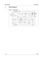
Block diagram TDA7410ND 6/34 1 Block diagram Figure 1. Block diagram Input Multiplexer Volume Bass & Treble OutLR OutLF OutRR OutRF 80kHz LP PLL & Pilot Detector Demodulator & Stereo Blend & Stereo Adjust 25kHz LP S & H High Cut Control Mute Noise Blanker Pulse Generator A D Supply Digital Control I2C Bus CDL CDG CDR Out_LR Out_LF Out_RR Out_RF SCL SDA GND CREF LEVEL VDD MPX AUX_L AUX_R CASS_R CASS_L AM Mute Loudness 8 1 2 6 7 9 15 14 20 5 4 3 11 17 19 16 18 12 13 10
Open the catalog to page 6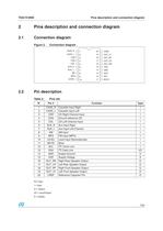
TDA7410ND Pins description and connection diagram 7/34 2 Pins description and connection diagram 2.1 Connection diagram Figure 2. Connection diagram 2.2 Pin description Pin Type: I = input O = Output I/O = Input/Output S = Supply 1 2 3 4 5 6 7 8 9 10 11 12 13 14 15 16 17 18 19 CASS_R 20 CASS_L CDR CDG CDL AUX_R AUX_L AM MPX LEVEL CREF OUT_LF OUT_RF OUT_LR OUT_RR VDD GND SDA SCL MUTE Table 2. Pins list N° Pin # Function Type 1 CASS_R Cassette Input Right I 2 CASS_L Cassette Input Left I 3 CDR CD Right Channel Input I 4 CDG Ground reference CD I 5 CDL CD Left Channel Input I 6 AUX_R Aux Input Right...
Open the catalog to page 7
Audio Processor Part TDA7410ND 8/34 3 Audio Processor Part Input Multiplexer œ Quasi-differential CD œ Cassette stereo and Aux stereo input œ AM mono and MPX œ Input gain stage with auto zero function Volume Control œ 1dB attenuator œ Max. gain 32dB œ Max. attenuation 79dB œ Softstep function Treble œ 2nd order frequency response œ Fixed center frequency 12.5kHz œ 7x2dB steps Bass Control œ 2nd order frequency response œ Fixed center frequency 100Hz œ DC gain programmable œ 7x 2dB steps œ Softstep function Speaker control œ 4 independent speaker controls (control range 50dB) œ Speaker mute Mute...
Open the catalog to page 8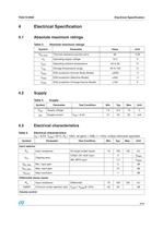
TDA7410ND Electrical Specification 9/34 4 Electrical Specification 4.1 Absolute maximum ratings 4.2 Supply 4.3 Electrical characteristics Table 3. Absolute maximum ratings Symbol Parameter Value Unit Rth-j pins Thermal resistance junction-pins 85 °C/W VS Operating supply voltage 10.5 V Tamb Operating ambient temperature -40 to 85 °C Tstg Storage temperature range -55 to 150 °C VESD ESD protection (Human Body Model) ±2000 V VESD ESD protection (Machine Model) ±200 V VESD ESD protection (Change Device Model) ±750 V Table 4. Supply Symbol Parameter Test Condition Min Typ Max Unit VDD Supply voltage...
Open the catalog to page 9
Electrical Specification TDA7410ND 10/34 GMAX Max gain 32 dB AMAX Max attenuation -83 -79 -75 dB ASTEP Step resolution -0.5 1 1.5 dB EA Attenuation set error G = -20 to +15dB 0 dB G = -79 to -20dB -4 0 3 dB ET Tracking error 2 dB VDC DC steps Adjacent attenuation steps 0.1 3 mV From 0dB to GMIN 0.5 5 mV Bass control Fc Center frequency fC 90 100 110 Hz Q 1.3 1.5 1.7 CRANGE Control range ±13 ±14 ±15 dB ASTEP Step resolution 1 2 3 dB DCGAIN Bass-DC-gain DC = off -1 0 1 dB DC = on 3.5 4.4 5.5 dB Treble control CRANGE Clipping level ±13 ±14 ±15 dB ASTEP Step resolution 1 2 3 dB fc Center frequency...
Open the catalog to page 10All STMicroelectronics catalogs and technical brochures
 STGW30NC60KD
14 Pages
 STGB14NC60K STGD14NC60K
16 Pages
 HD1750FX
8 Pages
 TDA75610SLV
42 Pages
 TDA7391
13 Pages
 TDA7376B
15 Pages
 TDA7375V
15 Pages
 TDA2005
25 Pages
 L4989D, L4989MD
19 Pages
 L4938ED L4938EPD
20 Pages
 L4949ED-E L4949EP-E
19 Pages
 L4925
L492514 Pages
 FDA903U
80 Pages
 FDA803U
76 Pages
 FDA903D
82 Pages
 FDA803D
78 Pages
 BALF-SPI2-02D3
13 Pages
 LIS2DTW12
65 Pages
 VL53L0X
40 Pages
 LPS22HH
59 Pages
 Standard products offer overview
13 Pages
 M40SZ100W
20 Pages
 A1C15S12M3
17 Pages
 TSX923
32 Pages
 TS1851
24 Pages
 LMV321
17 Pages
 Serial real-time clock (RTC) ICs
16 Pages
 TDA2003LG
8 Pages
 HCF4541 Programmable Timer
10 Pages
 STA8058 GPS multi-chip module
14 Pages
 TDA7410ND Signal Processor
34 Pages
 TSA1204 DUAL CHANNEL
31 Pages


Archived catalogs
 NEATSwitch
6 Pages
 Power MOSFETs for metering
2 Pages


- Single-pole switch
- Acceleration sensor
- Pressure probe
- Technology switch
- Signal amplifying integrated circuit
- Multipole switch
- Piezoelectric accelerometer
- Transceiver module
- Electronic filter
- Electromechanical switch
- Membrane pressure sensor
- Analog pressure sensor
- Rotary electric switch
- Triaxial acceleration sensor
- Power amplifying integrated circuit
- Distance sensor
- Diode
- STMicroelectronics transistor
- Low-pass electronic filter
- Absolute pressure sensor