
Catalog excerpts
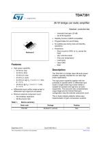
TDA7391 35 W bridge car radio amplifier Datasheet - production data – Internally fixed gain (30 dB) – No SVR Capacitor Standby function (CMOS compatible) Programmable turn-on/off delay No audible pop during mute and standby operations Protections: – Short circuit (to GND, to VS, across the load) – Very inductive loads – Chip over temperature – Load dump – Open GND – ESD Features High power capability: – 40 W/4 max – 35 W/4 EIAJ – 45 W/3.2 max – 40 W/3.2 EIAJ – 32 W/3.2 @ VS = 14.4 V, f = 1 kHz, d = 10 % – 26 W/4 @ VS = 14.4 V, f = 1 kHz, d = 10 % DIfferential inputs (either single ended or differential input signal are accepted) Minimum external component count: – No bootstrap capacitors – No Boucherot cells Table 1. Description The TDA7391 is a bridge class AB audio power amplifier specially intended for car radio high power applications. The high power capability together with the possibility to operate either in differential input mode or single ended input mode makes it suitable for boosters and high end car radio equipments. The exclusive fully complementary output stage and the internal fixed gain configuration drop the external component count. The on board clipping detector allows easy implementation of gain compression systems. Device summary Order code September 2013 This is information on a prod
Open the catalog to page 1
Block and pin description diagrams . . . . . . . . . . . . . . . . . . . . . . . . . . . . 5 1.1 1.2 Block diagram . . . . . . . . . . . . . . . . . . . . . . . . . . . . . . . . . . . . . . . . . . . . . . . 5 Pin description . . . . . . . . . . . . . . . . . . . . . . . . . . . . . . . . . . . . . . . . . . . . . . 5 Absolute maximum ratings . . . . . . . . . . . . . . . . . . . . . . . . . . . . . . . . . . . . . 7 Electrical characteristics curves . . . . . . . . . . . . . . . . . . . . . . . . . . . . . . . . . 9
Open the catalog to page 2
List of tables Table 1. Table 2. Table 3. Table 4. Table 5. Table 6. Device summary . . . . . . . . . . . . . . . . . . . . . . . . . . . . . . . . . . . . . . . . . . . . . . . . . . . . . . . . . . 1 Pin functional description . . . . . . . . . . . . . . . . . . . . . . . . . . . . . . . . . . . . . . . . . . . . . . . . . . . 6 Absolute maximum ratings . . . . . . . . . . . . . . . . . . . . . . . . . . . . . . . . . . . . . . . . . . . . . . . . . . 7 Thermal data. . . . . . . . . . . . . . . . . . . . . . . . . . . . . . . . . . . . . . . . . . . . . . . . . . . . . . . . . . . . . 7...
Open the catalog to page 3
List of figures Figure 1. Figure 2. Figure 3. Figure 4. Figure 5. Figure 6. Figure 7. Figure 8. Figure 9. Figure 10. Figure 11. Figure 12. Figure 13. Figure 14. Figure 15. Block diagram . . . . . . . . . . . . . . . . . . . . . . . . . . . . . . . . . . . . . . . . . . . . . . . . . . . . . . . . . . . . 5 Pin connection (top view) . . . . . . . . . . . . . . . . . . . . . . . . . . . . . . . . . . . . . . . . . . . . . . . . . . . 5 Test and application circuit . . . . . . . . . . . . . . . . . . . . . . . . . . . . . . . . . . . . . . . . . . . . . . . . . . 8 Printed circuit board and...
Open the catalog to page 4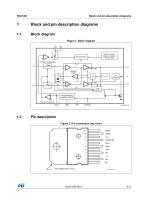
Block and pin description diagrams Block and pin description diagrams Block diagram Figure 1. Block diagram Pin description Figure 2. Pin connection (top view)
Open the catalog to page 5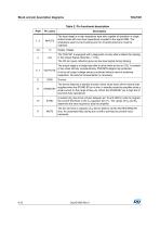
Block and pin description diagrams TDA7391 Table 2. Pin functional description Description The input stage is a high impedance type also capable of operation in single ended mode with one input capacitively coupled to the signal GND. The impedance seen by the inverting and non inverting input pins must be matched. Supply voltage. The TDA7391 is equipped with a diagnostic circuitry able to detect the clipping in the Output Signal (distortion = 10%). The CD pin (open collector) gives out low level signal during clipping. The output stage is a bridge type able to drive loads as low as 3.2. It...
Open the catalog to page 6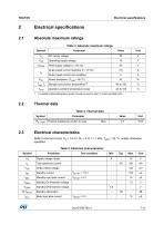
Electrical specifications Electrical specifications Absolute maximum ratings Table 3. Absolute maximum ratings Symbol Operating supply voltage Peak supply voltage (t = 50 ms) Output peak current repetitive (f > 10 Hz) Output peak current non repetitive Power dissipation (Tcase = 85 °C) VPEAK IO Ptot Tstg, Tj Tamb Operative ambient temperature range 1. A suitable heatsink/dissipation system should be used to keep Tj inside specified limits. Thermal data Table 4. Thermal data Symbol Rth j-case Parameter Thermal resistance junction to case Electrical characteristics Refer to the test circuit,...
Open the catalog to page 7
Electrical specifications TDA7391 Table 5. Electrical characteristics (continued) Test condition Mute attenuation Output power EIAJ output power Voltage gain High frequency roll-off Single Ended Input Impedance Input noise voltage Input common mode rejection Supply voltage rejection Clipping detection level Absolute thermal shutdown junction temperature 1. Saturated square wave output. Figure 3. Test and application circuit
Open the catalog to page 8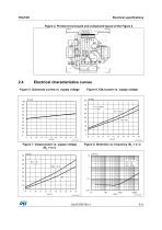
Electrical specifications Figure 4. Printed circuit board and component layout of the Figure 4 Electrical characteristics curves Figure 5. Quiescent current vs. supply voltage Figure 6. EIAJ power vs. supply voltage Figure 7. Output power vs. supply voltage (RL = 4 ) Figure 8. Distortion vs. frequency (RL = 4 )
Open the catalog to page 9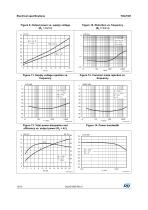
Electrical specifications Figure 9. Output power vs. supply voltage (RL = 3.2 ) Figure 10. Distortion vs. frequency (RL = 3.2 ) Figure 11. Supply voltage rejection vs. frequency Figure 12. Common mode rejection vs. frequency Figure 13. Total power dissipation and efficiency vs. output power (RL = 4) Figure 14. Power bandwidth
Open the catalog to page 10
Package information Package information In order to meet environmental requirements, ST offers these devices in different grades of ECOPACK® packages, depending on their level of environmental compliance. ECOPACK® specifications, grade definitions and product status are available at: www.st.com. ECOPACK® is an ST trademark Figure 15. Multiwatt11 (vertical) mechanical data and package dimensions
Open the catalog to page 11All STMicroelectronics catalogs and technical brochures
-
STGW30NC60KD
14 Pages
-
STGB14NC60K STGD14NC60K
16 Pages
-
HD1750FX
8 Pages
-
TDA75610SLV
42 Pages
-
TDA7376B
15 Pages
-
TDA7375V
15 Pages
-
TDA2005
25 Pages
-
L4989D, L4989MD
19 Pages
-
L4938ED L4938EPD
20 Pages
-
L4949ED-E L4949EP-E
19 Pages
-
L4925
14 Pages
-
FDA903U
80 Pages
-
FDA803U
76 Pages
-
FDA903D
82 Pages
-
FDA803D
78 Pages
-
BALF-SPI2-02D3
13 Pages
-
LIS2DTW12
65 Pages
-
VL53L0X
40 Pages
-
LPS22HH
59 Pages
-
Standard products offer overview
13 Pages
-
M40SZ100W
20 Pages
-
A1C15S12M3
17 Pages
-
TSX923
32 Pages
-
TS1851
24 Pages
-
LMV321
17 Pages
-
Serial real-time clock (RTC) ICs
16 Pages
-
TDA2003LG
8 Pages
-
HCF4541 Programmable Timer
10 Pages
-
STA8058 GPS multi-chip module
14 Pages
-
TDA7410ND Signal Processor
34 Pages
-
TDA7410ND Signal Processor
34 Pages
-
TSA1204 DUAL CHANNEL
31 Pages
Archived catalogs
-
NEATSwitch
6 Pages
-
Power MOSFETs for metering
2 Pages


