- Catalogs
- STMicroelectronics
- TDA7376B
TDA7376B
1 /15Pages

TDA7376B
1 /15Pages
Catalog excerpts
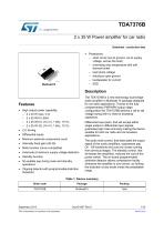
TDA7376B 2 x 35 W Power amplifier for car radio Datasheet - production data Protections: – short circuit (out to ground, out to supply voltage, across the load) – overrating chip temperature with soft thermal limiter – load dump voltage – fortuitous open ground – loudspeaker dc current – ESD Description The TDA7376B is a new technology dual bridge audio amplifier in Multiwatt 15 package designed for car radio applications. Thanks to the fully complementary PNP/NPN output stage configuration the TDA7376B delivers a rail-to-rail voltage swing with no need of bootstrap capacitors. Features High output power capability: – 2 x 40 W max./ 4 – 2 x 35 W/4 EIAJ – 2 x 25 W/4 (14.4 V, 1 kHz, 10 %) – 2 x 25 W/ 2 (14.4 V, 1 kHz, 10 %) Differential input pairs, that will accept either single ended or differential input signals, guarantee high noise immunity making the device suitable for both car radio and car boosters applications. 2 driving Differential inputs Minimum external components count Internally fixed gain (26 db) Mute function (cmos compatible) Automute at minimum supply voltage detection Standby function No audible pop during mute and standby operations Clipping detector with programmable distortion threshold The audio mute control, that attenuates the output signal of the audio amplifiers, suppresses pop On - Off transients and cuts any noises coming from previous stages. The standby control, that de-biases the amplifiers, reduces the cost of the power switch. The on-board programmable distortion detector allows compression facility whenever the amplifier is over driven, so limiting the distortion at any levels inside the presettable range. Table 1. Device summary Order code September 2013 This is information on a product in f
Open the catalog to page 1
Block and pin connection diagrams . . . . . . . . . . . . . . . . . . . . . . . . . . . . 5 1.1 Test and application circuits . . . . . . . . . . . . . . . . . . . . . . . . . . . . . . . . . . 7 Absolute maximum ratings . . . . . . . . . . . . . . . . . . . . . . . . . . . . . . . . . . . . . 9 Electrical characteristics curves . . . . . . . . . . . . . . . . . . . . . . . . . . . . . . . . .11
Open the catalog to page 2
List of tables Table 1. Table 2. Table 3. Table 4. Table 5. Device summary . . . . . . . . . . . . . . . . . . . . . . . . . . . . . . . . . . . . . . . . . . . . . . . . . . . . . . . . . . 1 Absolute maximum ratings . . . . . . . . . . . . . . . . . . . . . . . . . . . . . . . . . . . . . . . . . . . . . . . . . . 9 Thermal data. . . . . . . . . . . . . . . . . . . . . . . . . . . . . . . . . . . . . . . . . . . . . . . . . . . . . . . . . . . . . 9 Electrical characteristics . . . . . . . . . . . . . . . . . . . . . . . . . . . . . . . . . . . . . . . . . . . . . . . . . . . . 9 Document revision...
Open the catalog to page 3
List of figures Figure 1. Figure 2. Figure 3. Figure 4. Figure 5. Figure 6. Figure 7. Figure 8. Figure 9. Figure 10. Figure 11. Figure 12. Figure 13. Figure 14. Figure 15. Figure 16. Figure 17. Figure 18. Figure 19. Block diagram . . . . . . . . . . . . . . . . . . . . . . . . . . . . . . . . . . . . . . . . . . . . . . . . . . . . . . . . . . . . 5 Pin connection diagram (top view) . . . . . . . . . . . . . . . . . . . . . . . . . . . . . . . . . . . . . . . . . . . . 6 Differential inputs test and application circuit . . . . . . . . . . . . . . . . . . . . . . . . . . . . . . . . . . . . 7...
Open the catalog to page 4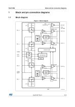
Block and pin connection diagrams Block and pin connection diagrams Block diagram Figure 1. Block diagram
Open the catalog to page 5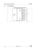
Block and pin connection diagrams Pin connection Figure 2. Pin connection diagram (top view)
Open the catalog to page 6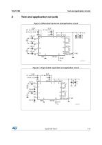
Test and application circuits Test and application circuits Figure 3. Differential inputs test and application circuit Figure 4. Single ended inputs test and application circuit
Open the catalog to page 7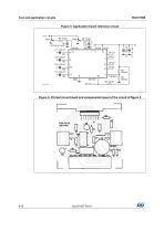
Test and application circuits TDA7376B Figure 5. Application board reference circuit Figure 6. Printed circuit board and components layout of the circuit of figure 5
Open the catalog to page 8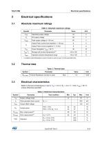
Electrical specifications Electrical specifications Absolute maximum ratings Table 2. Absolute maximum ratings Symbol Power Dissipation Tcase = 85 °C Output Peak Current (repetitive f > 10 Hz) Output Peak Current (not repetitive t = 100 s) Peak supply voltage (t = 50 ms) Operating supply voltage Operative ambient temperature range 1. A suitable heatsink/dissipation system should be used to keep Tj inside specified limits. Thermal data Table 3. Thermal data Symbol Thermal Resistance Junction to case Electrical characteristics Refer to the test circuits figures 3 and 4, VS = 14.4 V; RL = 4 ;...
Open the catalog to page 9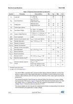
Electrical specifications TDA7376B Table 4. Electrical characteristics (continued) Test condition Cross talk Input Impedance differential input Single Ended input Voltage gain differential input Single Ended input Channel gain balance Input Noise Voltage Supply Voltage Rejection Power bandwidth Common mode rejection ratio VCM = 1 Vrms input referred Standby Attenuation Standby current consumption Mute attenuation Distortion detection level(2) Output low, sinked current Distortion detector output dc current Output high, leakage current (Vpin10 = VS, @ VSmax = 18V) 1. Saturated square wave output....
Open the catalog to page 10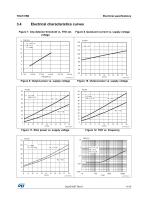
Electrical specifications Electrical characteristics curves Figure 7. Clip detector threshold vs. THD set. voltage Figure 8. Quiescent current vs. supply voltage Figure 9. Output power vs. supply voltage Figure 10. Output power vs. supply voltage Figure 11. EIAJ power vs. supply voltage
Open the catalog to page 11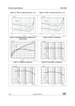
Electrical specifications Figure 13. THD vs. output power (RL = 4 ) Figure 14. THD vs. output power (RL = 2 ) Figure 15. Dissipated power & efficiency vs. output power Figure 17. CMRR vs. frequency Figure 18. Crosstalk vs. frequency
Open the catalog to page 12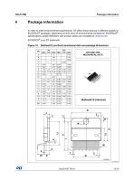
Package information Package information In order to meet environmental requirements, ST offers these devices in different grades of ECOPACK® packages, depending on their level of environmental compliance. ECOPACK® specifications, grade definitions and product status are available at: www.st.com. ECOPACK® is an ST trademark Figure 19. Multiwatt15 (vertical) mechanical data and package dimensions
Open the catalog to page 13All STMicroelectronics catalogs and technical brochures
 STGW30NC60KD
14 Pages
 STGB14NC60K STGD14NC60K
16 Pages
 HD1750FX
8 Pages
 TDA75610SLV
42 Pages
 TDA7391
13 Pages
 TDA7375V
15 Pages
 TDA2005
25 Pages
 L4989D, L4989MD
19 Pages
 L4938ED L4938EPD
20 Pages
 L4949ED-E L4949EP-E
19 Pages
 L4925
L492514 Pages
 FDA903U
80 Pages
 FDA803U
76 Pages
 FDA903D
82 Pages
 FDA803D
78 Pages
 BALF-SPI2-02D3
13 Pages
 LIS2DTW12
65 Pages
 VL53L0X
40 Pages
 LPS22HH
59 Pages
 Standard products offer overview
13 Pages
 M40SZ100W
20 Pages
 A1C15S12M3
17 Pages
 TSX923
32 Pages
 TS1851
24 Pages
 LMV321
17 Pages
 Serial real-time clock (RTC) ICs
16 Pages
 TDA2003LG
8 Pages
 HCF4541 Programmable Timer
10 Pages
 STA8058 GPS multi-chip module
14 Pages
 TDA7410ND Signal Processor
34 Pages
 TDA7410ND Signal Processor
34 Pages
 TSA1204 DUAL CHANNEL
31 Pages


Archived catalogs
 NEATSwitch
6 Pages
 Power MOSFETs for metering
2 Pages


- Single-pole switch
- Acceleration sensor
- Pressure probe
- Technology switch
- Signal amplifying integrated circuit
- Multipole switch
- Piezoelectric accelerometer
- Transceiver module
- Electronic filter
- Electromechanical switch
- Membrane pressure sensor
- Analog pressure sensor
- Rotary electric switch
- Triaxial acceleration sensor
- Distance sensor
- Diode
- STMicroelectronics transistor
- Low-pass electronic filter
- Absolute pressure sensor