
Catalog excerpts
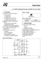
TDA7375V 2 x 35W dual/quad power amplifier for car radio 1 ■ HIGH OUTPUT POWER CAPABILITY: – 2 x 40W max./4 – 2 x 35W/4 EIAJ – 2 x 35W/4 EIAJ – 2 x 25W/4 @14.4V, 1KHz, 10% – 4 x 7W/4 @14.4V,1KHz, 10% – 4 x 12W/2 @14.4V, 1KHz, 10% MINIMUM EXTERNAL COMPONENTS COUNT: – NO BOOTSTRAP CAPACITORS – NO BOUCHEROT CELLS – INTERNALLY FIXED GAIN (26dB BTL) ST-BY FUNCTION (CMOS COMPATIBLE) Table 1. Order Codes Part Number NO AUDIBLE POP DURING ST-BY OPERATIONS CLIPPING OUT TO GND SHORT OUT TO VS SHORT SOFT SHORT AT TURN-ON THERMAL SHUTDOWN PROXIMITY PROTECTIONS: OUPUT AC/DC SHORT CIRCUIT – TO GND – TO VS – ACROSS THE LOAD SOFT SHORT AT TURN-ON OVERRATING CHIP TEMPERATURE WITH SOFT THERMAL LIMITER LOAD DUMP VOLTAGESURGE VERY INDUCTIVE LOADS FORTUITOUS OPEN GND REV
Open the catalog to page 1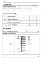
The TDA7375V is a new technology class AB car radio amplifier able to work either in DUAL BRIDGE or QUAD SINGLE ENDED configuration. The exclusive fully complementary structure of the output stage and the internally fixed gain guarantees the highest possible power performances with extremely reduced component count. The on-board clip detector simplifies gain compression operation. The fault diagnostics makes it possible to detect mistakes during car radio set assembly and wiring in the car. Table 2. Absolute Maximum Ratings Symbol Operating Supply Voltage Peak Supply Voltage (for t = 50ms)...
Open the catalog to page 2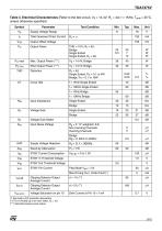
TDA7375V Table 4. Electrical Characteristcs (Refer to the test circuit, VS = 14.4V; RL = 4; f = 1KHz; Tamb = 25°C, unless otherwise specified) Symbol Total Quiescent Drain Current Test Condition Supply Voltage Range Output Power EIAJ Output Power (***) RL = 4 Single Ended, PO = 0.1 to 4W Bridge, PO = 0.1 to 10W Cross Talk THD = 10%; RL = 4 Bridge Single Ended Single Ended, RL = 2 Output Offset Voltage Input Noise Voltage Single Ended Voltage Gain Match Voltage Gain Single Ended Bridge Input Impedance Rg = 0; ”A” weighted, S.E. Non Inverting Channels Inverting Channels Supply Voltage...
Open the catalog to page 3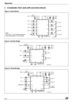
STANDARD TEST AND APPLICATION CIRCUIT Figure 4. Quad Stereo 10K R1 ST-BY C7 10μF IN FL Note: C9, C10, C11, C12 could be reduced if the 2W operation is not required. Figure 5. Double Bridge 10K R1 ST-BY C5 10μF IN L Figure 6. Stereo/Bridge 10K ST-BY
Open the catalog to page 4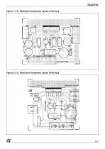
TDA7375V Figure 7. P.C. Board and Component Layout of the fig.4 Figure 8. P.C. Board and Component Layout of the fig.5
Open the catalog to page 5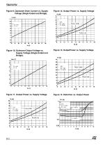
TDA7375V Figure 9. Quiescent Drain Current vs. Supply Voltage (Single Ended and Bridge). Figure 12. Output Power vs. Supply Voltage Figure 10. Quiescent Output Voltage vs. Supply Voltage (Single Ended and Bridge). Figure 13. OutputPower vs. Supply Voltage Figure 11. Output Power vs. Supply Voltage Figure 14. Distortion vs. Output Power
Open the catalog to page 6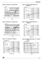
TDA7375V Figure 15. Distortion vs. Output Power Figure 18. Supply Voltage Rejection vs. Frequency Figure 16. Distortion vs. Output Power Figure 19. Supply Voltage Rejection vs. Frequency Figure 17. Cross-talk vs. Frequency Figure 20. Stand-by Attenuation vs. Threshold Voltage
Open the catalog to page 7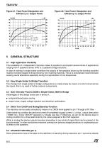
TDA7375V Figure 21. Total Power Dissipation and Efficiency vs. Output Power Figure 22. Total Power Dissipation and Efficiency vs. Output Power GENERAL STRUCTURE 5.1 High Application Flexibility The availability of 4 independent channels makes it possible to accomplish several kinds of applications ranging from 4 speakers stereo (F/R) to 2 speakers bridge solutions. In case of working in single ended conditions the polarity of the speakers driven by the inverting amplifier must be reversed respect to those driven by non inverting channels. This is to avoid phase inconveniences causing sound...
Open the catalog to page 8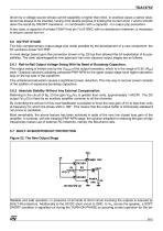
TDA7375V driven by a voltage source whose current capability is higher than 5mA. In practical cases a series resistance has always to be inserted, having it the double purpose of limiting the current at pin 7 and to smooth down the stand-by ON/OFF transitions - in combination with a capacitor - for output pop prevention. In any case, a capacitor of at least 100nF from pin 7 to S-GND, with no resistance in between, is necessary to ensure correct turn-on. 5.6 OUTPUT STAGE The fully complementary output stage was made possible by the development of a new component: the ST exclusive power ICV...
Open the catalog to page 9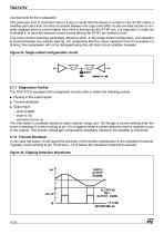
TDA7375V vice itself and for the loudspeaker. This particular kind of protection acts in a way to avoid that the device is turned on (by ST-BY) when a resistive path (less than 16 ohms) is present between the output and GND. As the involved circuitry is normally disabled when a current higher than 5mA is flowing into the ST-BY pin, it is important, in order not to disable it, to have the external current source driving the ST-BY pin limited to 5mA. This extra function becomes particularly attractive when, in the single ended configuration, one capacitor is shared between two outputs (see...
Open the catalog to page 10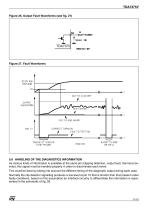
TDA7375V Figure 26. Output Fault Waveforms (see fig. 27) Figure 27. Fault Waveforms 5.8 HANDLING OF THE DIAGNOSTICS INFORMATION As various kinds of information is available at the same pin (clipping detection, output fault, thermal proximity), this signal must be handled properly in order to discriminate each event. This could be done by taking into account the different timing of the diagnostic output during each case. Normally the clip detector signalling produces a low level at pin 10 that is shorter than that present under faulty conditions; based on this assumption an interface...
Open the catalog to page 11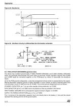
Figure 29. Interface circuitry to differentiate the information schematic 5.9 PCB-LAYOUT GROUNDING (general rules) The device has 2 distinct ground leads, P-GND (POWER GROUND) and S-GND (SIGNAL GROUND) which are practically disconnected from each other at chip level. Proper operation requires that P-GND and S-GND leads be connected together on the PCB-layout by means of reasonably low-resistance tracks. As for the PCB-ground configuration, a star-like arrangement whose center is represented by the supplyfiltering electrolytic capacitor ground is highly advisable. In such context, at least 2...
Open the catalog to page 12All STMicroelectronics catalogs and technical brochures
-
STGW30NC60KD
14 Pages
-
STGB14NC60K STGD14NC60K
16 Pages
-
HD1750FX
8 Pages
-
TDA75610SLV
42 Pages
-
TDA7391
13 Pages
-
TDA7376B
15 Pages
-
TDA2005
25 Pages
-
L4989D, L4989MD
19 Pages
-
L4938ED L4938EPD
20 Pages
-
L4949ED-E L4949EP-E
19 Pages
-
L4925
14 Pages
-
FDA903U
80 Pages
-
FDA803U
76 Pages
-
FDA903D
82 Pages
-
FDA803D
78 Pages
-
BALF-SPI2-02D3
13 Pages
-
LIS2DTW12
65 Pages
-
VL53L0X
40 Pages
-
LPS22HH
59 Pages
-
Standard products offer overview
13 Pages
-
M40SZ100W
20 Pages
-
A1C15S12M3
17 Pages
-
TSX923
32 Pages
-
TS1851
24 Pages
-
LMV321
17 Pages
-
Serial real-time clock (RTC) ICs
16 Pages
-
TDA2003LG
8 Pages
-
HCF4541 Programmable Timer
10 Pages
-
STA8058 GPS multi-chip module
14 Pages
-
TDA7410ND Signal Processor
34 Pages
-
TDA7410ND Signal Processor
34 Pages
-
TSA1204 DUAL CHANNEL
31 Pages
Archived catalogs
-
NEATSwitch
6 Pages
-
Power MOSFETs for metering
2 Pages


