- Catalogs
- STMicroelectronics
- TDA2005
TDA2005
1 /25Pages

TDA2005
1 /25Pages
Catalog excerpts
TDA2005 20 W bridge/stereo amplifier for car radio Datasheet production data High output power: – Po = 10 + 10 W @ RL = 2 , THD = 10 % – Po = 20 W @ RL = 4 , THD = 10 %. Protection against: – Output DC and AC short circuit to ground – Overrating chip temperature – Load dump voltage surge – Fortuitous open ground – Very inductive loads Loudspeaker protection during short circuit for one wire to ground Description The TDA2005 is a class B dual audio power amplifier in Multiwatt11 package specifically designed for car radio applications. Table 1. Power booster amplifiers can be easily designed using this device that provides a high current capability (up to 3.5 A) and can drive very low impedance loads (down to 1.6 in stereo applications) obtaining an output power of more than 20 W (bridge configuration). Device summary Order code September 2013 This is information on a product in full production.
Open the catalog to page 1
Schematic and pins connection diagrams . . . . . . . . . . . . . . . . . . . . . . . 5 Absolute maximum ratings . . . . . . . . . . . . . . . . . . . . . . . . . . . . . . . . . . . . . 6 Bridge amplifier section . . . . . . . . . . . . . . . . . . . . . . . . . . . . . . . . . . . . . . . 6 2.3.1 2.3.2 Electrical characteristics (bridge application) . . . . . . . . . . . . . . . . . . . . . . 7 Bridge amplifier design . . . . . . . . . . . . . . . . . . . . . . . . . . . . . . . . . . . . . . 9 Stereo amplifier application . . . . . . . . . . . . . . . . . . . . . . . . . . . . . . . . . . ....
Open the catalog to page 2
List of tables Table 1. Table 2. Table 3. Table 4. Table 5. Table 6. Table 7. Table 8. Table 9. Device summary . . . . . . . . . . . . . . . . . . . . . . . . . . . . . . . . . . . . . . . . . . . . . . . . . . . . . . . . . . 1 Absolute maximum ratings . . . . . . . . . . . . . . . . . . . . . . . . . . . . . . . . . . . . . . . . . . . . . . . . . . 6 Thermal data. . . . . . . . . . . . . . . . . . . . . . . . . . . . . . . . . . . . . . . . . . . . . . . . . . . . . . . . . . . . . 6 Electrical characteristics (bridge application) . . . . . . . . . . . . . . . . . . . . . . . . . . . . . ....
Open the catalog to page 3
List of figures Figure 1. Figure 2. Figure 3. Figure 4. Figure 5. Figure 6. Figure 7. Figure 8. Figure 9. Figure 10. Figure 11. Figure 12. Figure 13. Figure 14. Figure 15. Figure 16. Figure 17. Figure 18. Figure 19. Figure 20. Figure 21. Figure 22. Figure 23. Figure 24. Figure 25. Figure 26. Figure 27. Figure 28. Figure 29. Figure 30. Figure 31. Figure 32. Figure 33. Figure 34. Figure 35. Figure 36. Figure 37. Figure 38. Figure 39. Figure 40. Schematic diagram . . . . . . . . . . . . . . . . . . . . . . . . . . . . . . . . . . . . . . . . . . . . . . . . . . . . . . . . 5 Pins connection diagram...
Open the catalog to page 4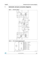
Schematic and pins connection diagrams Schematic and pins connection diagrams Figure 1. Schematic diagram Pins connection diagram (top view)
Open the catalog to page 5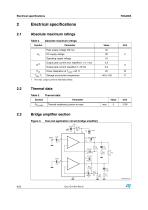
Electrical specifications Electrical specifications Absolute maximum ratings Table 2. Absolute maximum ratings Peak supply voltage (50 ms) Operating supply voltage Output peak current (non repetitive t = 0.1 ms) Output peak current (repetitive f 10 Hz) Power dissipation at Tcase = 60 °C Storage and junction temperature 1. The max. output current is internally limited. Thermal data Table 3. Thermal data Symbol Rth-j-case Parameter Thermal resistance junction-to-case Bridge amplifier section Figure 3. Test and application circuit (bridge amplifier)
Open the catalog to page 6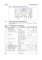
Electrical specifications Figure 4. PC board and components layout of Figure 3 Electrical characteristics (bridge application) Refer to the bridge application circuit Tamb = 25°C; Gv = 50dB; Rth(heatsink) = 4°C/W unless otherwise specified. Electrical characteristics (bridge application) Parameter Test condition Supply voltage Output offset voltage (between pin 8 and pin 10) Total quiescent drain current Output power Total harmonic distortion Input sensitivity Input resistance High frequency roll off (-3 dB) Closed loop voltage gain Total Input noise voltage Supply voltage rejection
Open the catalog to page 7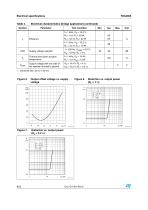
Electrical specifications Table 4. Electrical characteristics (bridge application) (continued) Test condition Supply voltage rejection Thermal shut-down junction temperature Output voltage with one side of the speaker shorted to ground Output offset voltage vs. supply voltage Distortion vs. output power (RL = 3.2 )
Open the catalog to page 8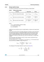
Electrical specifications Bridge amplifier design The following considerations can be useful when designing a bridge amplifier. Table 5. Bridge amplifier design Parameter Single ended Peak output voltage (before clipping) Peak Output current (before clipping) RMS output power (before clipping) Where: VCE sat = output transistors saturation voltage VS = allowable supply voltage RL = load impedance Voltage and current swings are twice for a bridge amplifier in comparison with single ended amplifier. In other words, with the same RL the bridge configuration can deliver an output power that is four...
Open the catalog to page 9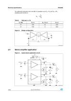
Electrical specifications For sufficiently high gains (40 to 50 dB) it is possible to put R2 = R4 and R3 = 2R1, simplifying the formula in: R1 G v = 4 -----R2 Table 6. Stereo amplifier application Figure 9. Bridge configuration Typical stereo application circuit
Open the catalog to page 10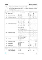
Electrical specifications Electrical characteristics (stereo application) Refer to the stereo application circuit Tamb = 25 °C; Gv = 50 dB; Rth(heatsink) = 4°C/W unless otherwise specified Electrical characteristics (stereo application) Test condition Supply voltage Quiescent offset voltage Total quiescent drain current Output power (each channel) Total harmonic distortion Cross talk Input saturation voltage Input sensitivity Input resistance High frequency roll off (-3 dB) Open loop voltage gain Gv Closed loop voltage gain
Open the catalog to page 11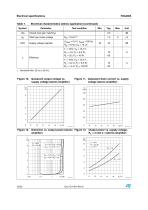
Electrical specifications Table 7. Electrical characteristics (stereo application) (continued) Test condition Closed loop gain matching Total input noise voltage Supply voltage rejection Figure 10. Quiescent output voltage vs. supply voltage (stereo amplifier) Figure 11. Quiescent drain current vs. supply voltage (stereo amplifier) Figure 12. Distortion vs. output power (stereo Figure 13. Output power vs. supply voltage, amplifier) RL = 2 and 4 (stereo amplifi
Open the catalog to page 12All STMicroelectronics catalogs and technical brochures
 STGW30NC60KD
14 Pages
 STGB14NC60K STGD14NC60K
16 Pages
 HD1750FX
8 Pages
 TDA75610SLV
42 Pages
 TDA7391
13 Pages
 TDA7376B
15 Pages
 TDA7375V
15 Pages
 L4989D, L4989MD
19 Pages
 L4938ED L4938EPD
20 Pages
 L4949ED-E L4949EP-E
19 Pages
 L4925
L492514 Pages
 FDA903U
80 Pages
 FDA803U
76 Pages
 FDA903D
82 Pages
 FDA803D
78 Pages
 BALF-SPI2-02D3
13 Pages
 LIS2DTW12
65 Pages
 VL53L0X
40 Pages
 LPS22HH
59 Pages
 Standard products offer overview
13 Pages
 M40SZ100W
20 Pages
 A1C15S12M3
17 Pages
 TSX923
32 Pages
 TS1851
24 Pages
 LMV321
17 Pages
 Serial real-time clock (RTC) ICs
16 Pages
 TDA2003LG
8 Pages
 HCF4541 Programmable Timer
10 Pages
 STA8058 GPS multi-chip module
14 Pages
 TDA7410ND Signal Processor
34 Pages
 TDA7410ND Signal Processor
34 Pages
 TSA1204 DUAL CHANNEL
31 Pages


Archived catalogs
 NEATSwitch
6 Pages
 Power MOSFETs for metering
2 Pages


- Single-pole switch
- Acceleration sensor
- Pressure probe
- Technology switch
- Signal amplifying integrated circuit
- Multipole switch
- Piezoelectric accelerometer
- Transceiver module
- Electronic filter
- Electromechanical switch
- Analog pressure sensor
- Membrane pressure sensor
- Rotary electric switch
- Triaxial acceleration sensor
- Distance sensor
- Diode
- Low-pass electronic filter
- Absolute pressure sensor