- Catalogs
- STMicroelectronics
- STGB8NC60KD - STGD8NC60KD STGF8NC60KD - STGP8NC60KD
STGB8NC60KD - STGD8NC60KD STGF8NC60KD - STGP8NC60KD
1 /18Pages

STGB8NC60KD - STGD8NC60KD STGF8NC60KD - STGP8NC60KD
1 /18Pages
Catalog excerpts

STGB8NC60KD - STGD8NC60KD STGF8NC60KD - STGP8NC60KD 600 V - 8 A - short circuit rugged IGBT Features ■ Lower on voltage drop (VCE(sat)) Lower CRES / CIES ratio (no cross-conduction susceptibility) Very soft ultra fast recovery antiparallel diode Short circuit withstand time 10 µs High frequency motor controls SMPS and PFC in both hard switch and resonant topologies Motor drivers Internal schematic diagram This IGBT utilizes the advanced PowerMESH™ process resulting in an excellent trade-off between switching performance and low on-state behavior. Device summary Order codes
Open the catalog to page 1
Electrical characteristics (curves) Test circuit Package mechanical data . . . . . . . . . . . . . . . . . . . . . . . . . . . . . . . . . . . . 11 Packaging mechanical data . . . . . . . . . . . . . . . . . . . . . . . . . . . . . . . . . . 15
Open the catalog to page 2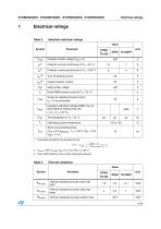
Electrical ratings Electrical ratings Table 2. Absolute maximum ratings Value Collector current (continuous) at TC = 25 °C Collector current (continuous) at TC = 100 °C Turn-off latching current Pulsed collector current Gate-emitter voltage Diode RMS forward current at TC = 25 °C Surge not repetitive forward current tp = 10 ms sinusoidal Insulation withstand voltage (RMS) from all three leads to external hea sink ( t=1 s; TC = 25 °C) Operating junction temperature Short circuit withstand time , (VCE = 0.5 VBR(CES) , TC = 125 °C, RG = 10 Ω VGE = 12 V) 1. Calculated according to the iterative formula:...
Open the catalog to page 3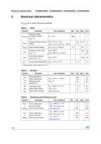
Electrical characteristics Electrical characteristics (TCASE=25°C unless otherwise specified) Table 4. Symbol Static Parameter Collector-emitter V(BR)CES breakdown voltage (VGE= 0) Test conditions Gate threshold voltage Collector cut-off current (VGE = 0) Collector-emitter saturation VGE= 15 V, IC = 3 A voltage VGE= 15 V, IC = 3 A, TC = 125°C Gate-emitter leakage current (VCE = 0) Forward transconductance 1. Pulse duration = 300 us, duty cycle 1.5 % Table 5. Symbol Cies Coes Cres Qg Qge Qgc Table 6. Symbol td(on) tr (di/dt)on td(on) tr (di/dt)on Dynamic Parameter Input capacitance Output capacitance...
Open the catalog to page 4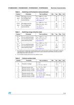
STGB8NC60KD - STGD8NC60KD - STGF8NC60KD - STGP8NC60KD Table 6. Symbol tr(Voff) td(off) tf tr(Voff) td(off) tf Electrical characteristics Switching on/off (inductive load) (continued) Parameter Off voltage rise time Turn-off delay time Current fall time Off voltage rise time Turn-off delay time Current fall time Test conditions Switching energy (inductive load) Parameter Turn-on switching losses Turn-off switching losses Total switching losses Turn-on switching losses Turn-off switching losses Total switching losses Test conditions 1. Eon is the turn-on losses when a typical diode is used in the...
Open the catalog to page 5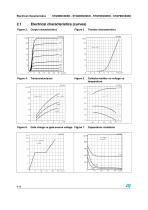
Electrical characteristics Electrical characteristics (curves) Output characteristics Transfer characteristics Collector-emitter on voltage vs temperature Gate charge vs gate-source voltage Figure 7. Capacitance variations
Open the catalog to page 6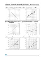
Normalized gate threshold voltage vs temperature Figure 10. Normalized breakdown voltage vs temperature Electrical characteristics Collector-emitter on voltage vs collector current Figure 11. Switching losses vs temperature Figure 12. Switching losses vs gate resistance Figure 13. Switching losses vs collector current
Open the catalog to page 7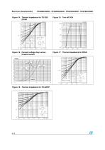
Electrical characteristics Figure 14. Thermal impedance for TO-220/ D²PAK Figure 16. Forward voltage drop versus forward current Figure 17. Thermal impedance for DPAK Figure 18. Thermal impedance for TO-220FP
Open the catalog to page 8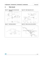
Test circuit Test circuit Figure 19. Test circuit for inductive load switching Figure 20. Gate charge test circuit Figure 21. Switching waveform Figure 22. Diode recovery time waveform
Open the catalog to page 9
Package mechanical data Package mechanical data In order to meet environmental requirements, ST offers these devices in ECOPACK® packages. These packages have a lead-free second level interconnect. The category of second level interconnect is marked on the package and on the inner box label, in compliance with JEDEC Standard JESD97. The maximum ratings related to soldering conditions are also marked on the inner box label. ECOPACK is an ST trademark. ECOPACK specifications are available at: www.st.com
Open the catalog to page 10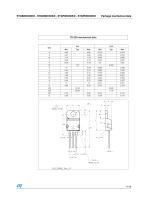
Package mechanical data
Open the catalog to page 11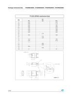
Package mechanical data TO-252 (DPAK) mechanical data DIM.
Open the catalog to page 12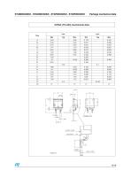
Package mechanical data D²PAK (TO-263) mechanical data
Open the catalog to page 13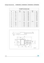
Package mechanical data
Open the catalog to page 14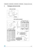
Packaging mechanical data Packaging mechanical data D2PAK FOOTPRINT TAPE AND REEL SHIPMENT REEL MECHANICAL DATA DIM. TAPE MECHANICAL DATA
Open the catalog to page 15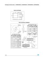
Packaging mechanical data DPAK FOOTPRINT TAPE AND REEL SHIPMENT REEL MECHANICAL DATA DIM. TAPE MECHANICAL DATA
Open the catalog to page 16
Revision history Revision history Table 9. Document revision history First release Updated Figure 14 and Figure 17
Open the catalog to page 17
Please Read Carefully: Information in this document is provided solely in connection with ST products. STMicroelectronics NV and its subsidiaries (“ST”) reserve the right to make changes, corrections, modifications or improvements, to this document, and the products and services described herein at any time, without notice. All ST products are sold pursuant to ST’s terms and conditions of sale. Purchasers are solely responsible for the choice, selection and use of the ST products and services described herein, and ST assumes no liability whatsoever relating to the choice, selection or use of...
Open the catalog to page 18All STMicroelectronics catalogs and technical brochures
 STGW30NC60KD
14 Pages
 STGB14NC60K STGD14NC60K
16 Pages
 HD1750FX
8 Pages
 TDA75610SLV
42 Pages
 TDA7391
13 Pages
 TDA7376B
15 Pages
 TDA7375V
15 Pages
 TDA2005
25 Pages
 L4989D, L4989MD
19 Pages
 L4938ED L4938EPD
20 Pages
 L4949ED-E L4949EP-E
19 Pages
 L4925
L492514 Pages
 FDA903U
80 Pages
 FDA803U
76 Pages
 FDA903D
82 Pages
 FDA803D
78 Pages
 BALF-SPI2-02D3
13 Pages
 LIS2DTW12
65 Pages
 VL53L0X
40 Pages
 LPS22HH
59 Pages
 Standard products offer overview
13 Pages
 M40SZ100W
20 Pages
 A1C15S12M3
17 Pages
 TSX923
32 Pages
 TS1851
24 Pages
 LMV321
17 Pages
 Serial real-time clock (RTC) ICs
16 Pages
 TDA2003LG
8 Pages
 HCF4541 Programmable Timer
10 Pages
 STA8058 GPS multi-chip module
14 Pages
 TDA7410ND Signal Processor
34 Pages
 TDA7410ND Signal Processor
34 Pages
 TSA1204 DUAL CHANNEL
31 Pages


Archived catalogs
 NEATSwitch
6 Pages
 Power MOSFETs for metering
2 Pages


- Single-pole switch
- Acceleration sensor
- Pressure probe
- Technology switch
- Signal amplifying integrated circuit
- Multipole switch
- Piezoelectric accelerometer
- Transceiver module
- Electronic filter
- Electromechanical switch
- Membrane pressure sensor
- Analog pressure sensor
- Rotary electric switch
- Triaxial acceleration sensor
- Power amplifying integrated circuit
- Distance sensor
- STMicroelectronics transistor
- Low-pass electronic filter
- Absolute pressure sensor