- Catalogs
- STMicroelectronics
- STA543SA 1x 24 W + 2 X 7 W triple amplifier with DC volume control
STA543SA 1x 24 W + 2 X 7 W triple amplifier with DC volume control
1 /23Pages

STA543SA 1x 24 W + 2 X 7 W triple amplifier with DC volume control
1 /23Pages
Catalog excerpts
PRELIMINARY DATA This is preliminary information on a new product now in development or undergoing evaluation. Details are subject to change without notice. Rev 2 July 2005 CD00061065 1/23 23 STA543SA 24W x 1 + 7W x 2 Triple Amplifier with DC Volume Control Features ¡ OUTPUT POWER CAPABILITY 24W x 1 + 7W x 2 @ VCC = 15V, RL = 4Ù, THD = 10% ¡ LINEAR DC VOLUME CONTROL FOR EACH SINGLE CHANNEL ¡ MINIMUM EXTERNAL COMPONENTS COUNT: – NO BOOTSTRAP CAPACITORS – NO BOUCHEROT CELLS – INTERNALLY FIXED GAIN (20dB SE, 26dB BTL) ¡ ST-BY FUNCTION (CMOS COMPATIBLE) ¡ NO AUDIBLE POP DURING ST-BY OPERATIONS ¡ DIAGNOSTIC FACILITIES – CLIP DETECTOR – OUT TO GND SHORT – OUT TO VS SHORT – SOFT SHORT AT TURN-ON – THERMAL SHUTDOWN PROXIMITY Protections ¡ OUPUT AC/DC SHORT CIRCUIT ¡ SOFT SHORT AT TURN-ON ¡ OVERRATING CHIP TEMPERATURE WITH SOFT THERMAL LIMITER ¡ VERY INDUCTIVE LOADS ¡ FORTUITOUS OPEN GND ¡ ESD Description The device is a class AB Audio amplifier assembled in the Clipwatt19 package; it is designed for high quality sound application. The STA543SA is a 3-channels audio amplifier with DC volume control dedicated for each single channel. It is a device suitable for 2.1 solution thank to its output configuration with two single ended channels and one bridge. The Short Circuit Protection, the Thermal Protection and the Diagnostics Functions are integrated in the device. Order codes Clipwatt 19 Part number Temp range, °C Package Packing STA543SA 0 to 70 Clipwatt 19 Tube www.st.com
Open the catalog to page 1
STA543SA 2/23 CD00061065 Contents 1 Block diagram and Pins description . . . . . . . . . . . . . . . . . . . . . . . . . . . . . . 4 1.1 Block diagram . . . . . . . . . . . . . . . . . . . . . . . . . . . . . . . . . . . . . . . . . . . . . . . . . 4 1.2 Pins description . . . . . . . . . . . . . . . . . . . . . . . . . . . . . . . . . . . . . . . . . . . . . . . 4 2 Electrical specifications . . . . . . . . . . . . . . . . . . . . . . . . . . . . . . . . . . . . . . . . 6 2.1 Absolute maximum ratings . . . . . . . . . . . . . . . . . . . . . . . . . . . . . . . . . . . . . . . 6 2.2 Thermal...
Open the catalog to page 2
STA543SA CD00061065 3/23 6 Thermal Information . . . . . . . . . . . . . . . . . . . . . . . . . . . . . . . . . . . . . . . . . . 20 6.1 Example (A): 2 channels Single Ended + 1Ch (BTL) . . . . . . . . . . . . . . . . . . 20 7 Package information . . . . . . . . . . . . . . . . . . . . . . . . . . . . . . . . . . . . . . . . . . 21 8 Revision history . . . . . . . . . . . . . . . . . . . . . . . . . . . . . . . . . . . . . . . . . . . . . . 22
Open the catalog to page 3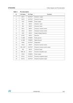
STA543SA 1 Block diagram and Pins description CD00061065 5/23 Table 1. Pin description N° Pin Name Pin Type Function 1 OUT1 OUTPUT Channel 1 output 2 OUT2 OUTPUT Channel 2 output 3 VCC POWER Power supply 4 IN1 INPUT Channel 1 input 5 IN2 INPUT Channel 2 input 6 VOL1 INPUT Channel 1 volume control 7 VOL2 INPUT Channel 2 volume control 8 SVR INPUT Supply Voltage Rejection 9 ST-BY INPUT Stand-by 10 P_GND POWER Power ground 11 S_GND POWER Signal Ground 12 DIAG OUTPUT Diagnostics 13 VOL3 INPUT Channel 3 volume control 14 VOL_OUT OUTPUT Channel 3 volume control output 15 IN3 INPUT Channel 3 input 16...
Open the catalog to page 5
2 Electrical specifications STA543SA 6/23 CD00061065 2 Electrical specifications 2.1 Absolute maximum ratings Table 2. Absolute maximum ratings 2.2 Thermal data Table 3. Thermal data 2.3 Electrical characteristics Symbol Parameter Value Unit Vop Operating Supply Voltage 18 V Vs DC Supply Voltage 20 V Ptot Total Power Dissipation (Tcase = 70°C) 35 W Tstg, Tj Storage and Junction Temperature -40 to150 °C Vctr Volume Control DC Voltage 7 V Top Operating Temperature 0 to 70 °C Symbol Parameter Value Unit Rth j-case Thermal Resistance Junction to case Max. 2 °C/W Rth j-amb Thermal Resistance Junction...
Open the catalog to page 6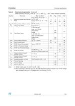
STA543SA 2 Electrical specifications CD00061065 7/23 Note: (*) DIAG Pulled-up to 5V with 10 kÙ; RL = 4Ù (**) For channel 3: if used the input pin 16 (with 100nF decoupling) instead of pin 15 the voltage gain is always max. and it is independent from Volume Control. Gv Maximum Voltage Gain Internally Fixed Single Ended, Vol Ctrl (Pins 6 and 7) > 4.5V Bridge, Vol Ctrl (pin 13) > 4.5V (**) 19 25 20 26 21 27 dB dB AMin Vol Attenuation at minimum volume Vol Ctrl < 0.5V 80 dB Gv Voltage Gain Match Single Ended 0.5 dB EN Total Output Noise f = 20 to 22 kHz (play, max. volume) Single Ended Bridge 500...
Open the catalog to page 7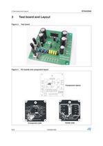
3 Test board and Layout STA543SA 8/23 CD00061065 3 Test board and Layout Figure 3. Test board Figure 4. PC boards and component layout Component side Solder side Component layout
Open the catalog to page 8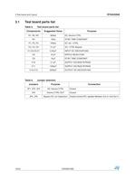
3 Test board and Layout STA543SA 10/23 CD00061065 3.1 Test board parts list Table 5. Test board parts list Components Suggested Value Purpose R1, R2, R3 300kÙ DC Volume CTRL R4 10kÙ ST-BY TIME CONSTANT P1, P2, P3 100kÙ DC Vol. -CTRL C2, C4, C6 0.1ìF Vol. -CTRL Bypass C1,C3,C5,C7 0.22ìF INPUT DC DECOUPLING C8 47ìF RIPPLE REJECTION C9 10ìF ST-BY TIME CONSTANT C10 0.1ìF SUPPLY VOLTAGE BYPASS C11 1000ìF SUPPLY VOLTAGE BYPASS C12,C13 2200ìF OUTPUT DC DECOUPLING Table 6. Jumper selection Jumpers Purpose Connection JP1, JP2, JP3 DC Volume CTRL Closed JP4 Volume CTRL OUT Closed JP5, JP6 Bypass DC out...
Open the catalog to page 10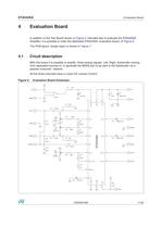
STA543SA 4 Evaluation Board CD00061065 11/23 4 Evaluation Board In addition to the Test Board shown in Figure 3. intended also to evaluate the STA540SA Amplifier, it is possible to order the dedicated STA543SA evaluation board of Figure 6. The PCB layout (single layer) is shown in Figure 7. 4.1 Crcuit description With this board it is possible to amplify three analog signals Left, Right, Subwoofer coming from separated sources or to generate the BASS part to be sent to the Subwoofer via a passive crossover network. All the three channels have a Linear DC volume Control. Figure 6. Evaluation Board...
Open the catalog to page 11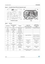
4 Evaluation Board STA543SA 12/23 CD00061065 Figure 7. Evaluation Board PCB and Component Layout Table 7. Part list Component Recommended Value Purpose Larger than Recommended value Smaller then Recommended value R1 10K St-By Circuit Larger On/Off time Smaller On/Off time R2,R7 Not mounted See notes R3,R6 Not mounted See notes R4,R5,R8 300K DC-Vol CTRL P1,P2 100K pot. DC-Vol CTRL R10 10K Open Collector Pull up C1 10uF St-by Circuit Larger On/Off time Smaller On/Off time C2 100nF Supply Voltage Bypass Danger of oscillations C3 1000uF Supply Voltage Bypass Danger of oscillations C4,C8 220nF Input...
Open the catalog to page 12All STMicroelectronics catalogs and technical brochures
 STGW30NC60KD
14 Pages
 STGB14NC60K STGD14NC60K
16 Pages
 HD1750FX
8 Pages
 TDA75610SLV
42 Pages
 TDA7391
13 Pages
 TDA7376B
15 Pages
 TDA7375V
15 Pages
 TDA2005
25 Pages
 L4989D, L4989MD
19 Pages
 L4938ED L4938EPD
20 Pages
 L4949ED-E L4949EP-E
19 Pages
 L4925
L492514 Pages
 FDA903U
80 Pages
 FDA803U
76 Pages
 FDA903D
82 Pages
 FDA803D
78 Pages
 BALF-SPI2-02D3
13 Pages
 LIS2DTW12
65 Pages
 VL53L0X
40 Pages
 LPS22HH
59 Pages
 Standard products offer overview
13 Pages
 M40SZ100W
20 Pages
 A1C15S12M3
17 Pages
 TSX923
32 Pages
 TS1851
24 Pages
 LMV321
17 Pages
 Serial real-time clock (RTC) ICs
16 Pages
 TDA2003LG
8 Pages
 HCF4541 Programmable Timer
10 Pages
 STA8058 GPS multi-chip module
14 Pages
 TDA7410ND Signal Processor
34 Pages
 TDA7410ND Signal Processor
34 Pages
 TSA1204 DUAL CHANNEL
31 Pages


Archived catalogs
 NEATSwitch
6 Pages
 Power MOSFETs for metering
2 Pages


- Bourn And Koch single-pole switch
- Bourn And Koch accelerometer
- Bourn And Koch pressure sensor
- Technology switch
- Bourn And Koch signal amplifier
- Multipole switch
- Piezoelectric accelerometer
- Bourn And Koch transceiver
- Bourn And Koch electronic filter
- Electromechanical switch
- Bourn And Koch membrane pressure sensor
- Bourn And Koch analog pressure sensor
- Rotary electric switch
- Triaxial acceleration sensor
- Bourn And Koch power amplifier
- Distance sensor
- Diode
- Bourn And Koch transistor
- Low-pass electronic filter
- Absolute pressure sensor