- Catalogs
- STMicroelectronics
- RHF1201 Rad-hard 12-bit 50 Msps A/D converter
RHF1201 Rad-hard 12-bit 50 Msps A/D converter
1 /34Pages

RHF1201 Rad-hard 12-bit 50 Msps A/D converter
1 /34Pages
Catalog excerpts
RHF1201 Rad-hard 12-bit 50 Msps A/D converter Features Failure immune (SEFI) and latchup immune (SEL) up to 120 MeV-cm2/mg at 2.7 V and 125° C Hermetic package Wide sampling range OptimwattTM adaptive power: 44 mW at 0.5 Msps, 100 mW at 50 Msps Optimized for 2 Vpp differential input Built-in reference voltage with external bias capability Digital communication satellites Space data acquisition systems Aerospace instrumentation Nuclear and high-energy physics The upper metallic lid is not electrically connected to any pins, nor to the IC die inside the package. Description The RHF1201 is a 12-bit 50 Msps sampling frequency analog-to-digital converter that uses pure (ELDRS-free) CMOS 0.25 µm technology combining high performance, radiation robustness and very low power consumption. The device is based on a pipeline structure and digital error correction to provide excellent static linearity. Specifically designed to optimize the speed power consumption ratio, the RHF1201 integrates a proprietary track-and-hold structure making it ideal for IF-sampling applications up to 150 MHz. A voltage reference network is integrated in the circuit to simplify the design and minimize external components. A tri-state capability is available on the outputs to allow common bus sharing. Output data can be coded in two different formats. A Data Ready signal, raised when the data is valid on the output, can be used for synchronization purposes. Quality level Engineering model Lead Packing finish Strip pack Strip pack 1. Contact your ST sales office for information about the specific conditions for products in die form and for information about SMD packages.
Open the catalog to page 1
Absolute maximum ratings and operating conditions . . . . . . . . . . . . . 9 Electrical characteristics (unchanged after 300 kRad) . . . . . . . . . . . . 10 7.1 Driving the analog input . . . . . . . . . . . . . . . . . . . . . . . . . . . . . . . . . . . . . . 21 Power consumption optimization . . . . . . . . . . . . . . . . . . . . . . . . . . . . . . . 27 Definitions of specified parameters . . . . . . . . . . . . . . . . . . . . . . . . . . . 29 8.1
Open the catalog to page 2
Block diagram Block diagram Figure 1. Block diagram Sequencer-phase shifting Digital data correction VCCBI VCCBE
Open the catalog to page 3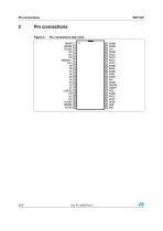
Figure 2. Pin connections (top view)
Open the catalog to page 4
Digital buffer ground Slew rate control input Digital buffer ground Output Enable input Digital buffer power supply Data Format Select input Analog power supply Analog power supply Out-of-range output Analog ground Most significant bit output Analog bias current input Digital output Digital output Bottom voltage reference Digital output Analog ground Digital output Analog input Digital output Analog ground Digital output Inverted analog input Digital output Analog ground Digital output Input common mode Digital output Analog ground Digital output Analog power supply Least significant bit output...
Open the catalog to page 5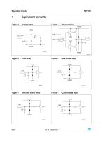
Equivalent circuits Equivalent circuits Analog inputs Output buffers VCCBE Clock input Data format input Slew rate control input Output enable input
Open the catalog to page 6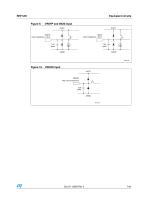
Equivalent circuits Figure 9. VREFP and INCM input AVCC INCM Input impedance = 50 Ω VREFP Input impedance = 39 Ω Figure 10. VREFM input AVCC VREFM High input impedance
Open the catalog to page 7
Timing characteristics Timing characteristics Table 3. Timing table Test conditions Data output delay (fall of clock to data valid) Data pipeline delay (2) Data ready rising edge delay Duty cycle = 50% after data change (3) Falling edge of OEB to digital output valid data Rising edge of OEB to digital output tri-state 1. See Figure 34. 2. Guaranteed by design. 3. Tdr is linked to the duty cycle, conditioned by the duration of the low level of DR signal. 4. See Figure 35 and Figure 36. Figure 11. Timing diagram N+2 Data output The input signal is sampled on the rising edge of the clock while the...
Open the catalog to page 8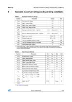
Absolute maximum ratings and operating conditions Absolute maximum ratings and operating conditions Table 4. Absolute maximum ratings Analog supply voltage Digital supply voltage Digital buffer supply voltage Digital buffer supply voltage Analog inputs: bottom limit −> top limit External references: bottom limit −> top limit VIN VINB VREFP VINCM IDout Digital output current Storage temperature Thermal resistance junction to case Thermal resistance junction to ambient 1. Human body model: a 100 pF capacitor is charged to the specified voltage, then discharged through a 1.5 kΩ resistor between...
Open the catalog to page 9
Electrical characteristics (unchanged after 300 kRad) Electrical characteristics (unchanged after 300 kRad) Unless otherwise specified, the test conditions in the following tables are: AVCC = DVCC = VCCBI = VCCBE = 2.5 V, FS = 50 Msps, differential input configuration, Fin = 15 MHz, VREFP = internal, VREFM = 0 V, Tamb = 25° C. Analog inputs Symbol VIN-VINB Test conditions Full-scale input differential voltage (FS)(2) Effective resolution bandwidth Input resistance Input capacitance 1. See Chapter 8: Definitions of specified parameters on page 29 for more information. 2. Optimized differential...
Open the catalog to page 10
Electrical characteristics (unchanged after 300 kRad) Digital inputs and outputs Test conditions Clock threshold Clock amplitude (DC component = 1.25 V) Square clock DVCC = 2.5 V High impedance leakage current Dynamic characteristics Parameter Test conditions Spurious free dynamic range Signal to noise ratio Total harmonics distortion F = 260 kHz Fs = 2 MHz Rpol = 200 k Ω each power supply at 2.5 V decoupled by 10 µF//470 nF Signal to noise and distortion ratio Effective number of bits Power supply rejection ratio
Open the catalog to page 11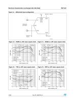
Electrical characteristics (unchanged after 300 kRad) Figure 12. Differential input configuration input signal Figure 13. ENOB vs. diff. input, square clock Figure 14. SINAD vs. diff. input, square clock Differential input Square clock Internal INCM and VREFP Differential input Square clock Internal INCM and VREFP Figure 15. THD vs. diff. input, square clock Figure 16. SNR vs. diff. input, square clock Differential input Square clock Internal INCM and VREFP Differential input Square clock Internal INCM and VREFP
Open the catalog to page 12All STMicroelectronics catalogs and technical brochures
 STGW30NC60KD
14 Pages
 STGB14NC60K STGD14NC60K
16 Pages
 HD1750FX
8 Pages
 TDA75610SLV
42 Pages
 TDA7391
13 Pages
 TDA7376B
15 Pages
 TDA7375V
15 Pages
 TDA2005
25 Pages
 L4989D, L4989MD
19 Pages
 L4938ED L4938EPD
20 Pages
 L4949ED-E L4949EP-E
19 Pages
 L4925
L492514 Pages
 FDA903U
80 Pages
 FDA803U
76 Pages
 FDA903D
82 Pages
 FDA803D
78 Pages
 BALF-SPI2-02D3
13 Pages
 LIS2DTW12
65 Pages
 VL53L0X
40 Pages
 LPS22HH
59 Pages
 Standard products offer overview
13 Pages
 M40SZ100W
20 Pages
 A1C15S12M3
17 Pages
 TSX923
32 Pages
 TS1851
24 Pages
 LMV321
17 Pages
 Serial real-time clock (RTC) ICs
16 Pages
 TDA2003LG
8 Pages
 HCF4541 Programmable Timer
10 Pages
 STA8058 GPS multi-chip module
14 Pages
 TDA7410ND Signal Processor
34 Pages
 TDA7410ND Signal Processor
34 Pages
 TSA1204 DUAL CHANNEL
31 Pages


Archived catalogs
 NEATSwitch
6 Pages
 Power MOSFETs for metering
2 Pages


- Bourn And Koch single-pole switch
- Bourn And Koch accelerometer
- Bourn And Koch pressure sensor
- Technology switch
- Bourn And Koch signal amplifier
- Multipole switch
- Piezoelectric accelerometer
- Bourn And Koch transceiver
- Bourn And Koch electronic filter
- Electromechanical switch
- Bourn And Koch membrane pressure sensor
- Bourn And Koch analog pressure sensor
- Rotary electric switch
- Triaxial acceleration sensor
- Bourn And Koch power amplifier
- Distance sensor
- Diode
- Bourn And Koch transistor
- Low-pass electronic filter
- Absolute pressure sensor