- Catalogs
- STMicroelectronics
- M40SZ100W
M40SZ100W
1 /20Pages

M40SZ100W
1 /20Pages
Catalog excerpts

M40SZ100W3 V NVRAM supervisor for LPSRAM Datasheet - production data Features • Convert low power SRAMs into NVRAMs • 3 V operating voltage • Precision power monitoring and power switching circuitry • Automatic write-protection when VCC is out-oftolerance • Choice of supply voltage and power-fail deselect voltage: - VCC = 2.7 to 3.6 V; 2.55 V < VPFD < 2.70 V • Reset output (RST) for power on reset • 1.25 V reference (for PFI/PFO) • Less than 15 ns chip enable access propagation delay • Battery low pin (BL) • RoHS compliant - Lead-free second level interconnect Description The M40SZ100W NVRAM controller is a self-contained device which converts a standard low-power SRAM into a non-volatile memory. A precision voltage reference and comparator monitors the VCC input for an out-of-tolerance condition. When an invalid VCC condition occurs, the conditioned chip enable output (ECON) is forced inactive to write protect the stored data in the SRAM. During a power failure, the SRAM is switched from the VCC pin to the external battery to provide the energy required for data retention. On a subsequent power-up, the SRAM remains write-protected until a valid power condition returns. This is information on a product in full production. www.stcom
Open the catalog to page 1
Data retention lifetime calculation . . . . . . . . . . . . . . . . . . . . . . . . . . . . . . . 8 Power-on reset output . . . . . . . . . . . . . . . . . . . . . . . . . . . . . . . . . . . . . . . 11 Reset input (RSTIN) . . . . . . . . . . . . . . . . . . . . . . . . . . . . . . . . . . . . . . . . . 11 VCC noise and negative going transients . . . . . . . . . . . . . . . . . . . . . . . . . 12 Package mechanical data . . . . . . . . . . . . . . . . . . . . . . . . . . . . . . . . . . . . 17
Open the catalog to page 2
List of tables Table 1. Table 2. Table 3. Table 4. Table 5. Table 6. Table 7. Table 8. Table 9. Table 10. Signal names . . . . . . . . . . . . . . . . . . . . . . . . . . . . . . . . . . . . . . . . . . . . . . . . . . . . . . . . . . . . 5 Power-down/up AC characteristics . . . . . . . . . . . . . . . . . . . . . . . . . . . . . . . . . . . . . . . . . . . 10 Reset AC characteristics. . . . . . . . . . . . . . . . . . . . . . . . . . . . . . . . . . . . . . . . . . . . . . . . . . . 11 Absolute maximum ratings . . . . . . . . . . . . . . . . . . . . . . . . . . . . . . . . . . . . . . . . ....
Open the catalog to page 3
List of figures Figure 1. Figure 2. Figure 3. Figure 4. Figure 5. Figure 6. Figure 7. Figure 8. Figure 9. Figure 10. Figure 11. Logic diagram . . . . . . . . . . . . . . . . . . . . . . . . . . . . . . . . . . . . . . . . . . . . . . . . . . . . . . . . . . . . 5 Pin connections . . . . . . . . . . . . . . . . . . . . . . . . . . . . . . . . . . . . . . . . . . . . . . . . . . . . . . . . . . 6 Block diagram . . . . . . . . . . . . . . . . . . . . . . . . . . . . . . . . . . . . . . . . . . . . . . . . . . . . . . . . . . . . 6 Hardware hookup . . . . . . . . . . . . . . . . . . . . . . . . ....
Open the catalog to page 4
Table 1. Signal names
Open the catalog to page 5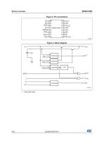
Device overview M40SZ100W Figure 2. Pin connections NC NC RST NC RSTIN PFO VBAT VSS Figure 3. Block diagram VOUT 1. Open drain output
Open the catalog to page 6
Device overview Figure 4. Hardware hookup 3.0V, 3.3V Regulator Unregulated Voltage M40SZ100W 0.1μF E From Microprocessor RSTIN To Battery Monitor Circuit
Open the catalog to page 7
Operation The M40SZ100W, as shown in Figure 4 on page 7, can control one (two, if placed in parallel) standard low-power SRAM. This SRAM must be configured to have the chip enable input disable all other input signals. Most slow, low-power SRAMs are configured like this, however many fast SRAMs are not. During normal operating conditions, the conditioned chip enable (ECON) output pin follows the chip enable (E) input pin with timing shown in Table 2 on page 10. An internal switch connects VCC to VOUT. This switch has a voltage drop of less than 0.3 V (IOUT1). When VCC degrades during a power...
Open the catalog to page 8
For a further more detailed review of lifetime calculations, please see application note AN1012. Figure 5. Power-down timing VCC VPFD (max) VPFD VPFD (min) VSO
Open the catalog to page 9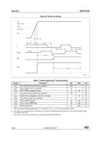
Table 2. Power-down/up AC characteristics 1. Valid for ambient operating temperature: Ta = -40 to 85 °C; Vcc = 2.7 to 3.6 V (except where noted). 2. VpFD (max) to VpFD (min) fall time of less than tF may result in deselection/write protection not occurring until 200 ps after Vcc passes VpFD (min). 3. VpFD (min) to Vss fall time of less than tFB may cause corruption of RAM data.
Open the catalog to page 10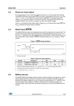
2.2 Power-on reset output All microprocessors have a reset input which forces them to a known state when starting. The M40SZ100W has a reset output (RST) pin which is guaranteed to be low by VPFD (see Table 7 on page 16). This signal is an open drain configuration. An appropriate pull-up resistor to VCC should be chosen to control the rise time. This signal will be valid for all voltage conditions, even when VCC equals VSS (with valid battery voltage). Once VCC exceeds the power failure detect voltage VPFD, an internal timer keeps RST low for tREC to allow the power supply to stabilize. 2.3 Reset...
Open the catalog to page 11
M40SZ100W If a battery low is generated during a power-up sequence, this indicates that the battery is below 2.5 V and may not be able to maintain data integrity in the SRAM. Data should be considered suspect, and verified as correct. A fresh battery should be installed. If a battery low indication is generated during the 24-hour interval check, this indicates that the battery is near end of life. However, data is not compromised due to the fact that a nominal VCC is supplied. In order to insure data integrity during subsequent periods of battery back-up mode, the battery should be replaced....
Open the catalog to page 12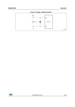
Operation Figure 8. Supply voltage protection VCC VCC
Open the catalog to page 13
Stressing the device above the rating listed in the absolute maximum ratings table may cause permanent damage to the device. These are stress ratings only and operation of the device at these or any other conditions above those indicated in the operating sections of this specification is not implied. Exposure to absolute maximum rating conditions for extended periods may affect device reliability. Table 4. Absolute maximum ratings 1. For SO package, Lead-free (Pb-free) lead finish: reflow at peak temperature of 260 °C (the time above 255 °C must not exceed 30 seconds). Caution: Negative undershoots...
Open the catalog to page 14All STMicroelectronics catalogs and technical brochures
 STGW30NC60KD
14 Pages
 STGB14NC60K STGD14NC60K
16 Pages
 HD1750FX
8 Pages
 TDA75610SLV
42 Pages
 TDA7391
13 Pages
 TDA7376B
15 Pages
 TDA7375V
15 Pages
 TDA2005
25 Pages
 L4989D, L4989MD
19 Pages
 L4938ED L4938EPD
20 Pages
 L4949ED-E L4949EP-E
19 Pages
 L4925
L492514 Pages
 FDA903U
80 Pages
 FDA803U
76 Pages
 FDA903D
82 Pages
 FDA803D
78 Pages
 BALF-SPI2-02D3
13 Pages
 LIS2DTW12
65 Pages
 VL53L0X
40 Pages
 LPS22HH
59 Pages
 Standard products offer overview
13 Pages
 A1C15S12M3
17 Pages
 TSX923
32 Pages
 TS1851
24 Pages
 LMV321
17 Pages
 Serial real-time clock (RTC) ICs
16 Pages
 TDA2003LG
8 Pages
 HCF4541 Programmable Timer
10 Pages
 STA8058 GPS multi-chip module
14 Pages
 TDA7410ND Signal Processor
34 Pages
 TDA7410ND Signal Processor
34 Pages
 TSA1204 DUAL CHANNEL
31 Pages


Archived catalogs
 NEATSwitch
6 Pages
 Power MOSFETs for metering
2 Pages


- Single-pole switch
- Acceleration sensor
- Pressure probe
- Technology switch
- Signal amplifying integrated circuit
- Multipole switch
- Piezoelectric accelerometer
- Transceiver module
- Electronic filter
- Electromechanical switch
- Membrane pressure sensor
- Analog pressure sensor
- Rotary electric switch
- Triaxial acceleration sensor
- Power amplifying integrated circuit
- Distance sensor
- Diode
- STMicroelectronics transistor
- Low-pass electronic filter
- Absolute pressure sensor