- Catalogs
- STMicroelectronics
- L9658 Octal squib driver and quad sensor interface ASIC for safety application
L9658 Octal squib driver and quad sensor interface ASIC for safety application
1 /64Pages

L9658 Octal squib driver and quad sensor interface ASIC for safety application
1 /64Pages
Catalog excerpts
L9658 Octal squib driver and quad sensor interface ASIC for safety application Features ■ 8 deployment drivers sized to deliver 1.2 A (min) for 2 ms (min) and 1.75 A (min) for 1 ms (min) Independently controlled high-side and lowside MOS for diagnosis Analog output available for resistance Squib short to ground, short to battery and MOS diagnostic available on SPI register Hall effect sensor support on satellite channels 3 and 4. Capability to deploy the squib with 1.2 A (min) or 1.75 A under 35 V load-dump condition and the low side MOS is shorted to ground Low voltage internal reset Package: 64 leads LQFP Capability to deploy the squib with 1.2 A (min) at 6.9 V VRES and 1.75 A at 12 V VRES Interface with 4 satellite sensors Programmable independent current trip points for each satellite channel Support Manchester protocol for satellite sensors Supports for variable bit rate detection Independent current limit and fault timer shutdown protection for each satellite output Squib drivers are sized to deploy 1.2 A minimum for 2 ms minimum during load dump and 1.75 A minimum for 1ms minimum during load dump. Short to ground and short to battery detection and reporting for each satellite channel Diagnostic of squib driver and squib resistance measurement is controlled by micro controller. Satellite message error detection Satellite interfaces support Manchester decoder with variable bit rate. Description L9658 is intended to deploy up to 8 squibs and to interface up to 4 satellites. 2 satellite interfaces can be used to interface Hall sensors. Device summary Order code
Open the catalog to page 1
Block diagram and application schematic . . . . . . . . . . . . . . . . . . . . . . . 7 1.1 1.2 Block diagram . . . . . . . . . . . . . . . . . . . . . . . . . . . . . . . . . . . . . . . . . . . . . . . 7 Application schematic . . . . . . . . . . . . . . . . . . . . . . . . . . . . . . . . . . . . . . . . . 7 Absolute maximum ratings . . . . . . . . . . . . . . . . . . . . . . . . . . . . . . . . . . . . 10 Serial peripheral interface (SPI) . . . . . . . . . . . . . . . . . . . . . . . . . . . . . . . . 19 4.8.1 4.8.2 Serial clock (SCLK, SCLK_A) . . . . . . . . . . . . . . . . . . . . . . ....
Open the catalog to page 2
High side MOS diagnostic . . . . . . . . . . . . . . . . . . . . . . . . . . . . . . . . . . . 30 Short to ground and open circuit . . . . . . . . . . . . . . . . . . . . . . . . . . . . . . 27 Deployment driver SPI bit definition . . . . . . . . . . . . . . . . . . . . . . . . . . . . . 32 4.11.1 4.11.2 Deployment driver register mode . . . . . . . . . . . . . . . . . . . . . . . . . . . . . . 33 Deployment driver command mode . . . . . . . . . . . . . . . . . . . . . . . . . . . . 34 Deployment driver diagnostic mode . . . . . . . . . . . . . . . . . . . . . . . . . . . . 35 Example of short...
Open the catalog to page 3
L9658 4.14.11 Satellite serial data input (MOSI) . . . . . . . . . . . . . . . . . . . . . . . . . . . . . . 52 4.14.12 Satellite MOSI bits definition . . . . . . . . . . . . . . . . . . . . . . . . . . . . . . . . . 52 4.14.13 Satellite module configuration register (CH1 only) . . . . . . . . . . . . . . . . 53 4.14.14 Channel configuration registers (CCR1, CCR2, CCR3, CCR4) . . . . . . . 54 4.14.15 SPI MISO Bits layout for configuration report . . . . . . . . . . . . . . . . . . . . 58
Open the catalog to page 4
List of tables Table 1. Table 2. Table 3. Table 4. Table 5. Table 6. Table 7. Table 8. Table 9. Table 10. Table 11. Table 12. Table 13. Table 14. Table 15. Table 16. Table 17. Table 18. Table 19. Table 20. Table 21. Table 22. Table 23. Table 24. Table 25. Table 26. Table 27. Table 28. Table 29. Table 30. Table 31. Table 32. Table 33. Table 34. Table 35. Table 36. Table 37. Table 38. Table 39. Table 40. Table 41. Table 42. Table 43. Table 44. Table 45. Table 46. Table 47. Table 48. Table 49. Device summary . . . . . . . . . . . . . . . . . . . . . . . . . . . . . . . . . . . . . . . . . . . ....
Open the catalog to page 5
List of figures Figure 1. Figure 2. Figure 3. Figure 4. Figure 5. Figure 6. Figure 7. Figure 8. Figure 9. Figure 10. Figure 11. Figure 12. Figure 13. Figure 14. Figure 15. Figure 16. Figure 17. Figure 18. Figure 19. Figure 20. Figure 21. Figure 22. Figure 23. Block diagram . . . . . . . . . . . . . . . . . . . . . . . . . . . . . . . . . . . . . . . . . . . . . . . . . . . . . . . . . . . . 7 Application schematic . . . . . . . . . . . . . . . . . . . . . . . . . . . . . . . . . . . . . . . . . . . . . . . . . . . . . . 7 MOS settling time and turn-on time 1 . . . . . . . . . . . . . . . . ....
Open the catalog to page 6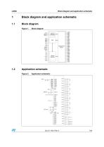
Block diagram and application schematic Block diagram and application schematic Block diagram Figure 1. Block diagram CS_A SCLK_A MOSI_A MISO_A Arming Interface CS_D CS_S SCLK MOSI MISO IREF VCC TEST DEPEN V8BUCK RESET AOUT Deployment Driver Sensor Interface Application schematic Figure 2. Application schematic VRES Reset pin of Power Supply RESETB CS_D CS_S SCLK MOSI MISO CS_A SCLK_A MOSI_A MISO_A DEPEN IF3/V3 IF4/V4 Satellite Sensor Satellite Sensor Satellite Sensor OR Hall Effect Switch Satellite Sensor OR Hall Effect Switch
Open the catalog to page 7
Pin function (continued) Pin name Reset state Supply voltage for satellite interface and resistance measurement Current sense output for channel 4 Current sense output for channel 3 Current sense output for channel 2 Current sense output for channel 1 No connect External current reference resistor AOUT_GND Ground reference for AOUT Analog output for loop diagnostics Power ground for loop channel 3 Low side driver output for channel 3 High side driver output for channel 3 Reserve voltage for loop channel 3 Reserve voltage for loop channel 2 High side driver output for channel 2 Low side driver...
Open the catalog to page 9
Electrical specification Electrical specification Maximum ratings The device may not operate properly if maximum operating condition is exceeded. Maximum operating conditions Discrete input voltage (RESETB, DEPEN, CS_A, CS_D, CS_S, SCLK, SCLK_A, MOSI, MOSI_A, MISO, MISO_A) Junction temperature Supply voltage Absolute maximum ratings Maximum ratings are absolute ratings; exceeding any one of these values may cause permanent damage to the integrated circuit. Absolute maximum ratings Supply voltage Discrete input voltage (RESETB, DEPEN, CS_A, CS_D, CS_S, SCLK, SCLK_A, MOSI, MOSI_A, MISO, MISO_A)...
Open the catalog to page 10All STMicroelectronics catalogs and technical brochures
 STGW30NC60KD
14 Pages
 STGB14NC60K STGD14NC60K
16 Pages
 HD1750FX
8 Pages
 TDA75610SLV
42 Pages
 TDA7391
13 Pages
 TDA7376B
15 Pages
 TDA7375V
15 Pages
 TDA2005
25 Pages
 L4989D, L4989MD
19 Pages
 L4938ED L4938EPD
20 Pages
 L4949ED-E L4949EP-E
19 Pages
 L4925
L492514 Pages
 FDA903U
80 Pages
 FDA803U
76 Pages
 FDA903D
82 Pages
 FDA803D
78 Pages
 BALF-SPI2-02D3
13 Pages
 LIS2DTW12
65 Pages
 VL53L0X
40 Pages
 LPS22HH
59 Pages
 Standard products offer overview
13 Pages
 M40SZ100W
20 Pages
 A1C15S12M3
17 Pages
 TSX923
32 Pages
 TS1851
24 Pages
 LMV321
17 Pages
 Serial real-time clock (RTC) ICs
16 Pages
 TDA2003LG
8 Pages
 HCF4541 Programmable Timer
10 Pages
 STA8058 GPS multi-chip module
14 Pages
 TDA7410ND Signal Processor
34 Pages
 TDA7410ND Signal Processor
34 Pages
 TSA1204 DUAL CHANNEL
31 Pages


Archived catalogs
 NEATSwitch
6 Pages
 Power MOSFETs for metering
2 Pages


- Single-pole switch
- Acceleration sensor
- Pressure probe
- Technology switch
- Signal amplifying integrated circuit
- Multipole switch
- Piezoelectric accelerometer
- Transceiver module
- Electronic filter
- Electromechanical switch
- Membrane pressure sensor
- Analog pressure sensor
- Rotary electric switch
- Triaxial acceleration sensor
- Power amplifying integrated circuit
- Distance sensor
- Diode
- STMicroelectronics transistor
- Low-pass electronic filter
- Absolute pressure sensor