- Catalogs
- STMicroelectronics
- L6390 High-voltage high and low side driver
L6390 High-voltage high and low side driver
1 /22Pages

L6390 High-voltage high and low side driver
1 /22Pages
Catalog excerpts
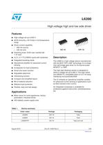
August 2010 Doc ID 14493 Rev 5 1/22 22 L6390 High-voltage high and low side driver Features ¡ High voltage rail up to 600 V ¡ dV/dt immunity ± 50 V/nsec in full temperature range ¡ Driver current capability: – 290 mA source, – 430 mA sink ¡ Switching times 75/35 nsec rise/fall with 1 nF load ¡ 3.3 V, 5 V TTL/CMOS inputs with hysteresis ¡ Integrated bootstrap diode ¡ Operational amplifier for advanced current sensing ¡ Comparator for fault protections ¡ Smart shut down function ¡ Adjustable dead-time ¡ Interlocking function ¡ Compact and simplified layout ¡ Bill of material reduction ¡ Effective fault protection ¡ Flexible, easy and fast design Applications ¡ Motor driver for home appliances, factory automation, industrial drives. ¡ HID ballasts, power supply units. Description The L6390 is a high-voltage device manufactured with the BCD “OFF-LINE” technology. It is a single chip half-bridge gate driver for N-channel power MOSFET or IGBT. The high side (floating) section is designed to stand a voltage rail up to 600 V. The logic inputs are CMOS/TTL compatible down to 3.3 V for easy interfacing microcontroller/DSP. The IC embeds an operational amplifier suitable for advanced current sensing in applications such as field oriented motor control. An integrated comparator is available for protections against overcurrent, overtemperature, etc. SO-16 DIP-16 Table 1. Device summary Order codes Package Packaging L6390N DIP-16 Tube L6390D SO-16 Tube L6390DTR SO-16 Tape and reel www.st.com
Open the catalog to page 1
Contents L6390 2/22 Doc ID 14493 Rev 5 Contents 1 Block diagram . . . . . . . . . . . . . . . . . . . . . . . . . . . . . . . . . . . . . . . . . . . . . . 3 2 Pin connection . . . . . . . . . . . . . . . . . . . . . . . . . . . . . . . . . . . . . . . . . . . . . . 4 3 Truth table . . . . . . . . . . . . . . . . . . . . . . . . . . . . . . . . . . . . . . . . . . . . . . . . . 5 4 Electrical data . . . . . . . . . . . . . . . . . . . . . . . . . . . . . . . . . . . . . . . . . . . . . . 6 4.1 Absolute maximum ratings . . . . . . . . . . . . . . . . . . . . . . . . . . . . . . . . . . . . . 6...
Open the catalog to page 2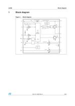
L6390 Block diagram Doc ID 14493 Rev 5 3/22 1 Block diagram Figure 1. Block diagram UV DETECTION LEVEL SHIFTER BOOTSTRAP DRIVER S VCC LVG DRIVER HIN LIN HVG DRIVER HVG BOOT OUT LVG UV DETECTION OP+ OPGND OPOUT SD/OD DT OPAMP DEAD TIME R LOGIC SHOOT THROUGH PREVENTION SD LATCH FLOATING STRUCTURE COMPARATOR + VREF CP+ 1 2 11 14 15 16 7 5 8 3 4 10 9 6 SMART SD from LVG VCC VCC 5V + - + - 5V
Open the catalog to page 3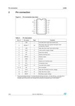
Pin connection L6390 4/22 Doc ID 14493 Rev 5 2 Pin connection Figure 2. Pin connection (top view) Table 2. Pin description Pin n # Pin name Type Function 1 LIN I Low side driver logic input (active low) 2 SD/OD (1) 1. The circuit provides less than 1 V on the LVG and HVG pins (@ Isink = 10 mA), with VCC > 3 V. This allows omitting the “bleeder” resistor connected between the gate and the source of the external MOSFET normally used to hold the pin low; the gate driver assures low impedance also in SD condition. I/O Shut down logic input (active low)/open drain (comparator output) 3 HIN I High...
Open the catalog to page 4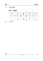
L6390 Truth table Doc ID 14493 Rev 5 5/22 3 Truth table Note: X: don't care Table 3. Truth table Input Output SD LIN HIN LVG HVG L X X L L H H L L L H L H L L H L L H L H H H L H
Open the catalog to page 5
Electrical data L6390 6/22 Doc ID 14493 Rev 5 4 Electrical data 4.1 Absolute maximum ratings Note: ESD immunity for pins 14, 15 and 16 is guaranteed up to 1 kV (human body model) 4.2 Thermal data Table 4. Absolute maximum rating Symbol Parameter Value Unit Min Max Vcc Supply voltage - 0.3 21 V Vout Output voltage Vboot - 21 Vboot + 0.3 V Vboot Bootstrap voltage - 0.3 620 V Vhvg High side gate output voltage Vout - 0.3 Vboot + 0.3 V Vlvg Low side gate output voltage - 0.3 Vcc + 0.3 V Vop+ OPAMP non-inverting input - 0.3 Vcc + 0.3 V Vop- OPAMP inverting input - 0.3 Vcc + 0.3 V Vcp+ Comparator input...
Open the catalog to page 6
L6390 Electrical data Doc ID 14493 Rev 5 7/22 4.3 Recommended operating conditions Table 6. Recommended operating conditions Symbol Pin Parameter Test condition Min Max Unit Vcc 4 Supply voltage 12.5 20 V VBO (1) 1. VBO = Vboot - Vout 16-14 Floating supply voltage 12.4 20 V Vout 14 DC output voltage - 9 (2) 2. LVG off. Vcc = 12.5 V Logic is operational if Vboot > 5 V Refer to AN2738 for more details 580 V fsw Switching frequency HVG, LVG load CL = 1 nF 800 kHz TJ Junction temperature -40 125 °C
Open the catalog to page 7
Electrical characteristics L6390 8/22 Doc ID 14493 Rev 5 5 Electrical characteristics 5.1 AC operation Table 7. AC operation electrical characteristics (VCC = 15 V; TJ = +25 °C) Symbol Pin Parameter Test condition Min Typ Max Unit ton 1 vs 11 3 vs 15 High/low side driver turn-on propagation delay Vout = 0 V Vboot = Vcc CL = 1 nF Vi = 0 to 3.3 V See Figure 3. 50 125 200 ns toff High/low side driver turn-off propagation delay 50 125 200 ns tsd 2 vs 11, 15 Shut down to high/low side driver propagation delay 50 125 200 ns tisd Comparator triggering to high/low side driver turn-off propagation delay...
Open the catalog to page 8
Electrical characteristics L6390 10/22 Doc ID 14493 Rev 5 5.2 DC operation Table 8. DC operation electrical characteristics (VCC = 15 V; TJ = + 25 °C) Symbol Pin Parameter Test condition Min Typ Max Unit Low supply voltage section Vcc_hys 4 Vcc UV hysteresis 1200 1500 1800 mV Vcc_thON Vcc UV turn ON threshold 11.5 12 12.5 V Vcc_thOFF Vcc UV turn OFF threshold 10 10.5 11 V Iqccu Undervoltage quiescent supply current Vcc = 10 V SD = 5 V; LIN = 5 V; HIN = GND; RDT = 0 Ù; CP+=OP+=GND; OP-=5 V 120 150 ìA Iqcc Quiescent current Vcc = 15 V SD = 5 V; LIN = 5 V; HIN = GND; RDT = 0 Ù; CP+=OP+=GND; OP-=5...
Open the catalog to page 10
L6390 Electrical characteristics Doc ID 14493 Rev 5 11/22 Vil 1, 2, 3 Low logic level voltage 0.8 V Vih High logic level voltage 2.25 V Vil_S 1, 3 Single input voltage LIN and HIN connected together and floating 0.8 V IHINh 3 HIN logic “1” input bias current HIN = 15 V 110 175 260 ìA IHINl HIN logic “0” input bias current HIN = 0 V 1 ìA ILINl 1 LIN logic “0” input bias current LIN = 0 V 3 6 20 ìA ILINh LIN logic “1” input bias current LIN = 15 V 1 ìA ISDh 2 SD logic “1” input bias current SD = 15 V 10 40 100 ìA ISDl SD logic “0” input bias current SD = 0 V 1 ìA 1. VBO = Vboot - Vout 2. RDSON...
Open the catalog to page 11All STMicroelectronics catalogs and technical brochures
 STGW30NC60KD
14 Pages
 STGB14NC60K STGD14NC60K
16 Pages
 HD1750FX
8 Pages
 TDA75610SLV
42 Pages
 TDA7391
13 Pages
 TDA7376B
15 Pages
 TDA7375V
15 Pages
 TDA2005
25 Pages
 L4989D, L4989MD
19 Pages
 L4938ED L4938EPD
20 Pages
 L4949ED-E L4949EP-E
19 Pages
 L4925
L492514 Pages
 FDA903U
80 Pages
 FDA803U
76 Pages
 FDA903D
82 Pages
 FDA803D
78 Pages
 BALF-SPI2-02D3
13 Pages
 LIS2DTW12
65 Pages
 VL53L0X
40 Pages
 LPS22HH
59 Pages
 Standard products offer overview
13 Pages
 M40SZ100W
20 Pages
 A1C15S12M3
17 Pages
 TSX923
32 Pages
 TS1851
24 Pages
 LMV321
17 Pages
 Serial real-time clock (RTC) ICs
16 Pages
 TDA2003LG
8 Pages
 HCF4541 Programmable Timer
10 Pages
 STA8058 GPS multi-chip module
14 Pages
 TDA7410ND Signal Processor
34 Pages
 TDA7410ND Signal Processor
34 Pages
 TSA1204 DUAL CHANNEL
31 Pages


Archived catalogs
 NEATSwitch
6 Pages
 Power MOSFETs for metering
2 Pages


- Single-pole switch
- Acceleration sensor
- Pressure probe
- Technology switch
- Signal amplifying integrated circuit
- Multipole switch
- Piezoelectric accelerometer
- Transceiver module
- Electronic filter
- Electromechanical switch
- Analog pressure sensor
- Membrane pressure sensor
- Rotary electric switch
- Triaxial acceleration sensor
- Power amplifying integrated circuit
- Distance sensor
- STMicroelectronics transistor
- Low-pass electronic filter
- Absolute pressure sensor